- 您现在的位置:买卖IC网 > PDF目录2063 > ADA4859-3ACPZ-RL (Analog Devices Inc)IC AMP 3CH CFB G=2 W/CP 16LFCSP PDF资料下载
参数资料
| 型号: | ADA4859-3ACPZ-RL |
| 厂商: | Analog Devices Inc |
| 文件页数: | 5/16页 |
| 文件大小: | 0K |
| 描述: | IC AMP 3CH CFB G=2 W/CP 16LFCSP |
| 标准包装: | 5,000 |
| 应用: | 电流反馈 |
| 电路数: | 3 |
| -3db带宽: | 265MHz |
| 转换速率: | 740 V/µs |
| 电流 - 电源: | 17mA |
| 电流 - 输出 / 通道: | 19mA |
| 电压 - 电源,单路/双路(±): | 3 V ~ 5.5 V |
| 安装类型: | 表面贴装 |
| 封装/外壳: | 16-VQFN 裸露焊盘,CSP |
| 供应商设备封装: | 16-LFCSP-VQ EP(4x4) |
| 包装: | 带卷 (TR) |
Data Sheet
ADA4859-3
Rev. A | Page 13 of 16
APPLICATIONS INFORMATION
USING THE ADA4859-3 IN GAINS EQUAL TO +1, 1
The ADA4859-3 was designed to offer outstanding video
performance, simplify applications, and minimize board area.
The ADA4859-3 is a triple amplifier with on-chip feedback
and gain set resistors. The gain is fixed internally at G = +2. The
inclusion of the on-chip resistors not only simplifies the design
of the application but also eliminates six surface-mount resistors,
saving valuable board space and lowering assembly costs.
Although the ADA4859-3 has a fixed gain of G = +2, it can be
used in other gain configurations, such as G = 1 and G = +1.
Unity-Gain Operation
Option 1
There are two options for obtaining unity gain (G = +1). The
first is shown in Figure 32. In this configuration, the IN input
pin is tied to the output. (Feedback is provided through the two
internal 550 resistors in parallel), and the input is applied to
the noninverting input. The noise gain for this configuration is 1.
0.1F
10F
VIN
RT
VOUT
+VS
GAIN OF +1
07715-
130
Figure 32. Unity Gain of Option 1
Option 2
Another option exists for running the ADA4859-3 as a unity-
gain amplifier. In this configuration, the noise gain is +2, see
Figure 33. The frequency response and transient response for
this configuration closely match the gain of +2 plots because the
noise gains are equal. This method does have twice the noise
gain of Option 1; however, in applications that do not require low
noise, Option 2 offers less peaking and ringing. By tying the inputs
together, the net gain of the amplifier becomes +1. Equation 1
shows the transfer characteristic for the schematic shown in
+
=
G
F
IN
G
F
IN
OUT
R
V
R
V
(1)
which simplifies to VOUT = VIN.
0.1F
VIN
RT
VOUT
+VS
GAIN OF +1
07715-
131
10F
RF
RG
Figure 33. Unity Gain of Option 2
Inverting Unity-Gain Operation
In this configuration, the noninverting input is tied to ground
and the input signal is applied to the inverting input. The noise
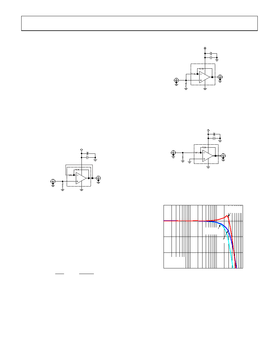
gain for this configuration is +2, see Figure 34.
0.01F
VIN
RT
VOUT
+VS
GAIN OF –1
07715-
132
10F
Figure 34. Inverting Configuration (G = 1)
Figure 35 shows the small signal frequency response for both
gain of +1 (Option 1 and Option 2) and gain of 1 configurations.
It is clear that the G = +1 Option 2 has better flatness and no
peaking compared to Option 1.
3
–9
–6
–3
0
1
10
100
1000
C
LOS
E
D
-LOOP
GA
IN
(
dB
)
FREQUENCY (MHz)
G = +1,
OPTION 1
G = +1,
OPTION 2
G = –1
07715-
031
VS = 5V
VOUT = 2V p-p
RL = 100
Figure 35. Large Signal, G = +1 and G = 1
相关PDF资料 |
PDF描述 |
|---|---|
| ADA4922-1ACPZ-R2 | IC ADC DRIVER 18BIT DIFF 8-LFCSP |
| ADA4937-2YCPZ-RL | IC ADC DRIVER DUAL DIFF 24LFCSP |
| ADA4938-2ACPZ-RL | IC ADC DRIVER DUAL DIFF 24LFCSP |
| ADA4941-1YRZ-R7 | IC DIFF ADC DRIVER 18BIT 8SOIC |
| ADA4960-1ACPZ-R2 | IC ADC DRIVER DIFF 16LFCSP |
相关代理商/技术参数 |
参数描述 |
|---|---|
| ADA4860-1 | 制造商:AD 制造商全称:Analog Devices 功能描述:High Speed, Low Cost, Op Amp |
| ADA4860-1YRJ-EBZ | 功能描述:BOARD EVAL FOR ADA4860-1YRJ RoHS:是 类别:编程器,开发系统 >> 评估板 - 运算放大器 系列:- 产品培训模块:Lead (SnPb) Finish for COTS Obsolescence Mitigation Program 标准包装:1 系列:- |
| ADA4860-1YRJZ-R2 | 制造商:Analog Devices 功能描述:OP Amp Single Current Fdbk 制造商:Analog Devices 功能描述:OP AMP SGL CURRENT FDBK 12V 6PIN SOT-23 - Tape and Reel 制造商:Analog Devices 功能描述:ANAADA4860-1YRJZ-R2 LOW COST CURRENT FEE |
| ADA4860-1YRJZ-RL | 功能描述:IC OPAMP CF LP 85MA SOT23-6 RoHS:是 类别:集成电路 (IC) >> Linear - Amplifiers - Instrumentation 系列:- 标准包装:160 系列:- 放大器类型:通用 电路数:4 输出类型:满摆幅 转换速率:10 V/µs 增益带宽积:9MHz -3db带宽:- 电流 - 输入偏压:1pA 电压 - 输入偏移:250µV 电流 - 电源:730µA 电流 - 输出 / 通道:28mA 电压 - 电源,单路/双路(±):2.7 V ~ 5.5 V,±1.35 V ~ 2.75 V 工作温度:-40°C ~ 125°C 安装类型:表面贴装 封装/外壳:16-SOIC(0.154",3.90mm 宽) 供应商设备封装:16-SOIC N 包装:管件 |
| ADA4860-1YRJZ-RL7 | 功能描述:IC OPAMP CF LP 85MA SOT23-6 RoHS:是 类别:集成电路 (IC) >> Linear - Amplifiers - Instrumentation 系列:- 产品培训模块:Differential Circuit Design Techniques for Communication Applications 标准包装:1 系列:- 放大器类型:RF/IF 差分 电路数:1 输出类型:差分 转换速率:9800 V/µs 增益带宽积:- -3db带宽:2.9GHz 电流 - 输入偏压:3µA 电压 - 输入偏移:- 电流 - 电源:40mA 电流 - 输出 / 通道:- 电压 - 电源,单路/双路(±):3 V ~ 3.6 V 工作温度:-40°C ~ 85°C 安装类型:表面贴装 封装/外壳:16-VQFN 裸露焊盘,CSP 供应商设备封装:16-LFCSP-VQ 包装:剪切带 (CT) 产品目录页面:551 (CN2011-ZH PDF) 其它名称:ADL5561ACPZ-R7CT |
发布紧急采购,3分钟左右您将得到回复。