- 您现在的位置:买卖IC网 > PDF目录2063 > ADA4859-3ACPZ-RL (Analog Devices Inc)IC AMP 3CH CFB G=2 W/CP 16LFCSP PDF资料下载
参数资料
| 型号: | ADA4859-3ACPZ-RL |
| 厂商: | Analog Devices Inc |
| 文件页数: | 6/16页 |
| 文件大小: | 0K |
| 描述: | IC AMP 3CH CFB G=2 W/CP 16LFCSP |
| 标准包装: | 5,000 |
| 应用: | 电流反馈 |
| 电路数: | 3 |
| -3db带宽: | 265MHz |
| 转换速率: | 740 V/µs |
| 电流 - 电源: | 17mA |
| 电流 - 输出 / 通道: | 19mA |
| 电压 - 电源,单路/双路(±): | 3 V ~ 5.5 V |
| 安装类型: | 表面贴装 |
| 封装/外壳: | 16-VQFN 裸露焊盘,CSP |
| 供应商设备封装: | 16-LFCSP-VQ EP(4x4) |
| 包装: | 带卷 (TR) |
ADA4859-3
Data Sheet
Rev. A | Page 14 of 16
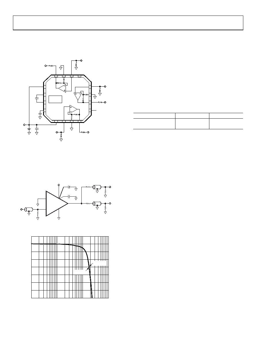
VIDEO LINE DRIVER
The ADA4859-3 was designed to excel in video driver applications.
Figure 36 shows a typical schematic for a video driver operating
on bipolar supplies.
07715-
134
1
2
3
4
11
12
CHARGE
PUMP
10
9
5
6
7
8
16
15
14
13
1F
+
10F
0.1F
+VS
1F
VIN (B)
75
VOUT (B)
75
VOUT (G)
75
VOUT (R)
75
VIN (G)
75
VIN (R)
PD
Figure 36. Video Driver Schematic
In applications that require multiple video loads be driven
simultaneously, the ADA4859-3 can deliver. Figure 37 shows
the ADA4859-3 configured with two video loads, and Figure 38
shows the large signal performance for multiple video loads.
07715-
135
75
CABLE
75
CABLE
75
VOUT2
VOUT1
+VS
0.1F
10F
VIN
75
CABLE
75
+
–
Figure 37. Video Driver Schematic for Two Video Loads
6.5
2.5
3.0
3.5
4.0
4.5
5.0
5.5
6.0
1
10
100
1000
C
LOS
E
D
-LOOP
GA
IN
(
dB
)
FREQUENCY (MHz)
RL = 150
RL = 75
07715-
034
Figure 38. Large Signal Frequency Response for Various Loads
POWER-DOWN
The ADA4859-3 is equipped with a PD (power-down) pin for
all three amplifiers. This allows the user the ability to reduce the
quiescent supply current when an amplifier is not active. The
power-down threshold levels are derived from ground level.
The amplifiers are powered down when the voltage applied to
the PD pin is greater than a certain voltage from ground. In a 5 V
supply application, the voltage is greater than 2 V, and in a 3.3 V
supply application, the voltage is greater than 1.5 V. The amplifier
is enabled whenever the PD pin is connected to ground. If the
PD pin is not used, it is best to connect it to ground. Note that
the power-down feature does not control the charge pump output
voltage and current.
Table 5. Power-Down Voltage Control
PD Pin
5 V
3.3 V
Not Active
<1.5 V
<1 V
Active
>2 V
>1.5 V
LAYOUT CONSIDERATIONS
As is the case with all high speed applications, careful attention
to printed circuit board (PCB) layout details prevents associated
board parasitics from becoming problematic. Proper RF design
technique is mandatory. The PCB should have a ground plane
covering all unused portions of the component side of the board to
provide a low impedance return path. Removing the ground
plane on all layers from the area near the input and output pins
reduces stray capacitance. Locate termination resistors and loads as
close as possible to their respective inputs and outputs. Keep
input and output traces as far apart as possible to minimize
coupling (crosstalk) through the board. Adherence to microstrip or
stripline design techniques for long signal traces (greater than
about 1 inch) is recommended.
POWER SUPPLY BYPASSING
Careful attention must be paid to bypassing the power supply pins
of the ADA4859-3. Use high quality capacitors with low equivalent
series resistance (ESR), such as multilayer ceramic capacitors
(MLCCs), to minimize supply voltage ripple and power dissipation.
A large, usually tantalum, 10 F to 47 F capacitor located in
proximity to the ADA4859-3 is required to provide good
decoupling for lower frequency signals. In addition, locate 0.1 F
MLCC decoupling capacitors as close to each of the power supply
pins as is physically possible, no more than 1/8-inch away. The
ground returns should terminate immediately into the ground
plane. Locating the bypass capacitor return close to the load
return minimizes ground loops and improves performance.
相关PDF资料 |
PDF描述 |
|---|---|
| ADA4922-1ACPZ-R2 | IC ADC DRIVER 18BIT DIFF 8-LFCSP |
| ADA4937-2YCPZ-RL | IC ADC DRIVER DUAL DIFF 24LFCSP |
| ADA4938-2ACPZ-RL | IC ADC DRIVER DUAL DIFF 24LFCSP |
| ADA4941-1YRZ-R7 | IC DIFF ADC DRIVER 18BIT 8SOIC |
| ADA4960-1ACPZ-R2 | IC ADC DRIVER DIFF 16LFCSP |
相关代理商/技术参数 |
参数描述 |
|---|---|
| ADA4860-1 | 制造商:AD 制造商全称:Analog Devices 功能描述:High Speed, Low Cost, Op Amp |
| ADA4860-1YRJ-EBZ | 功能描述:BOARD EVAL FOR ADA4860-1YRJ RoHS:是 类别:编程器,开发系统 >> 评估板 - 运算放大器 系列:- 产品培训模块:Lead (SnPb) Finish for COTS Obsolescence Mitigation Program 标准包装:1 系列:- |
| ADA4860-1YRJZ-R2 | 制造商:Analog Devices 功能描述:OP Amp Single Current Fdbk 制造商:Analog Devices 功能描述:OP AMP SGL CURRENT FDBK 12V 6PIN SOT-23 - Tape and Reel 制造商:Analog Devices 功能描述:ANAADA4860-1YRJZ-R2 LOW COST CURRENT FEE |
| ADA4860-1YRJZ-RL | 功能描述:IC OPAMP CF LP 85MA SOT23-6 RoHS:是 类别:集成电路 (IC) >> Linear - Amplifiers - Instrumentation 系列:- 标准包装:160 系列:- 放大器类型:通用 电路数:4 输出类型:满摆幅 转换速率:10 V/µs 增益带宽积:9MHz -3db带宽:- 电流 - 输入偏压:1pA 电压 - 输入偏移:250µV 电流 - 电源:730µA 电流 - 输出 / 通道:28mA 电压 - 电源,单路/双路(±):2.7 V ~ 5.5 V,±1.35 V ~ 2.75 V 工作温度:-40°C ~ 125°C 安装类型:表面贴装 封装/外壳:16-SOIC(0.154",3.90mm 宽) 供应商设备封装:16-SOIC N 包装:管件 |
| ADA4860-1YRJZ-RL7 | 功能描述:IC OPAMP CF LP 85MA SOT23-6 RoHS:是 类别:集成电路 (IC) >> Linear - Amplifiers - Instrumentation 系列:- 产品培训模块:Differential Circuit Design Techniques for Communication Applications 标准包装:1 系列:- 放大器类型:RF/IF 差分 电路数:1 输出类型:差分 转换速率:9800 V/µs 增益带宽积:- -3db带宽:2.9GHz 电流 - 输入偏压:3µA 电压 - 输入偏移:- 电流 - 电源:40mA 电流 - 输出 / 通道:- 电压 - 电源,单路/双路(±):3 V ~ 3.6 V 工作温度:-40°C ~ 85°C 安装类型:表面贴装 封装/外壳:16-VQFN 裸露焊盘,CSP 供应商设备封装:16-LFCSP-VQ 包装:剪切带 (CT) 产品目录页面:551 (CN2011-ZH PDF) 其它名称:ADL5561ACPZ-R7CT |
发布紧急采购,3分钟左右您将得到回复。