- 您现在的位置:买卖IC网 > PDF目录5875 > ADA4897-2ARMZ-R7 (Analog Devices Inc)IC OPAMP RR 230MHZ LP 10MSOP PDF资料下载
参数资料
| 型号: | ADA4897-2ARMZ-R7 |
| 厂商: | Analog Devices Inc |
| 文件页数: | 10/29页 |
| 文件大小: | 0K |
| 描述: | IC OPAMP RR 230MHZ LP 10MSOP |
| 标准包装: | 1,000 |
| 放大器类型: | 电压反馈 |
| 电路数: | 2 |
| 输出类型: | 满摆幅 |
| 转换速率: | 120 V/µs |
| -3db带宽: | 230MHz |
| 电流 - 输入偏压: | 11µA |
| 电压 - 输入偏移: | 28µV |
| 电流 - 电源: | 3mA |
| 电流 - 输出 / 通道: | 80mA |
| 电压 - 电源,单路/双路(±): | 3 V ~ 10 V,±1.5 V ~ 5 V |
| 工作温度: | -40°C ~ 125°C |
| 安装类型: | 表面贴装 |
| 封装/外壳: | 10-TFSOP,10-MSOP(0.118",3.00mm 宽) |
| 供应商设备封装: | 10-MSOP |
| 包装: | 带卷 (TR) |
第1页第2页第3页第4页第5页第6页第7页第8页第9页当前第10页第11页第12页第13页第14页第15页第16页第17页第18页第19页第20页第21页第22页第23页第24页第25页第26页第27页第28页第29页
Data Sheet
ADA4896-2/ADA4897-1/ADA4897-2
Rev.
| Page 17 of 28
THEORY OF OPERATION
AMPLIFIER DESCRIPTION
noise amplifiers that consume 3 mA from supplies ranging from
3 V to 10 V. Fabricated on the Analog Devices SiGe bipolar process,
excess of 200 MHz. The amplifiers are unity-gain stable, and the
input structure results in an extremely low input 1/f noise for a
high speed amplifier.
The rail-to-rail output stage is designed to drive the heavy feed-
back load required to achieve an overall low output referred noise.
To meet more demanding system requirements, the large signal
increased beyond the typical fundamental limits of other low noise,
unity-gain stable amplifiers. The maximum offset voltage of 500 μV
and drift of 0.2 μV/°C make the ADA4896-2/ADA4897-1/
ADA4897-2 excellent amplifier choices even when the low noise
performance is not needed because there is minimal power
penalty in achieving the low input noise or the high bandwidth.
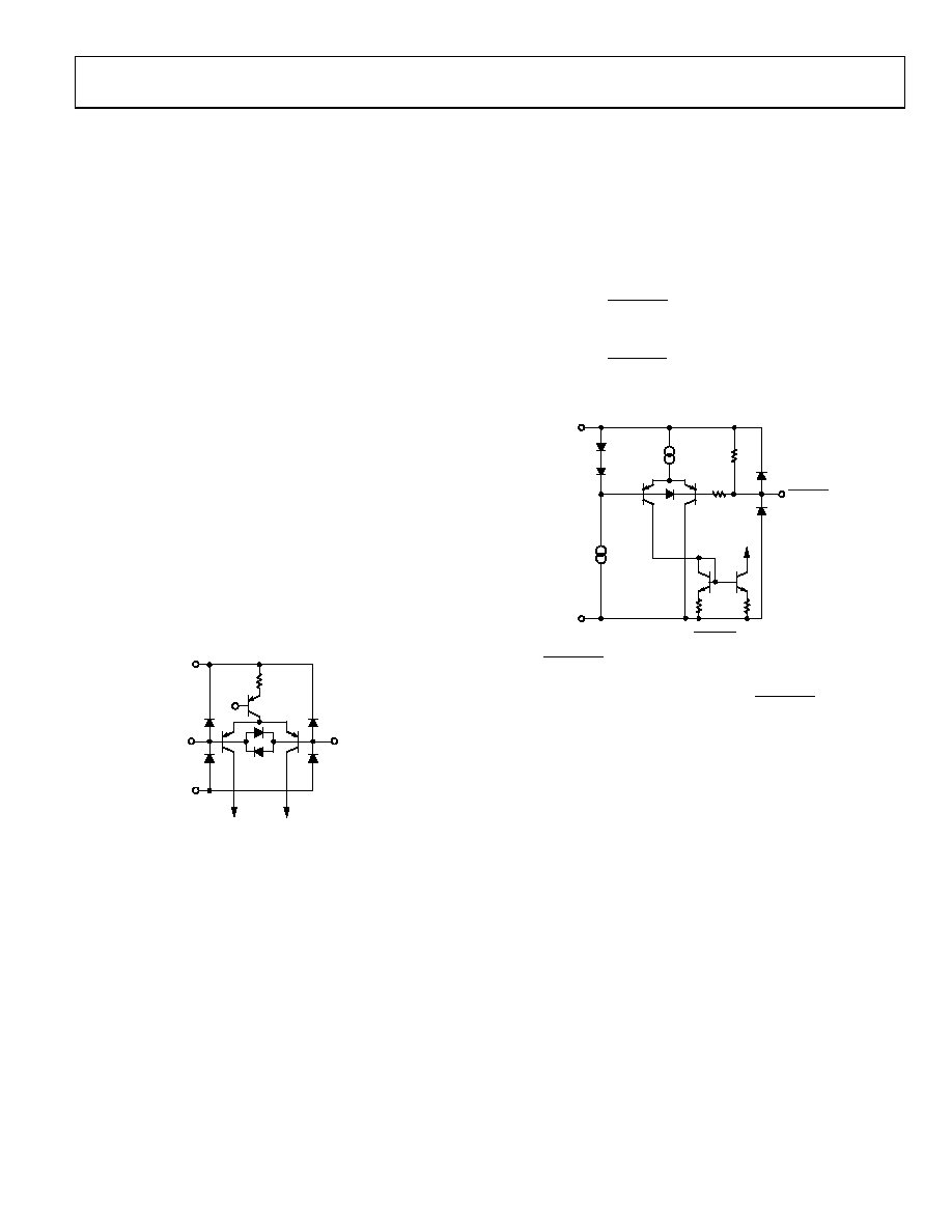
INPUT PROTECTION
from ESD events, withstanding human body model ESD events
of 2.5 kV and charged-device model events of 1 kV with no mea-
sured performance degradation. The precision input is protected
with an ESD network between the power supplies and diode
clamps across the input device pair, as shown in Figure 44.
+IN
ESD
–VS
+VS
BIAS
TO THE REST OF THE AMPLIFIER
–IN
ESD
09
44
7-
06
8
Figure 44. Input Stage and Protection Diodes
For differential voltages above approximately 0.7 V, the diode
clamps begin to conduct. Too much current can cause damage
due to excessive heating. If large differential voltages must be
sustained across the input terminals, it is recommended that the
current through the input clamps be limited to less than 10 mA.
Series input resistors that are sized appropriately for the expected
differential overvoltage provide the needed protection.
The ESD clamps begin to conduct for input voltages that are
more than 0.7 V above the positive supply and input voltages
more than 0.7 V below the negative supply. If an overvoltage
condition is expected, it is recommended that the input current
be limited to less than 10 mA.
DISABLE OPERATION
circuitry. If the DISABLE pin is left unconnected, the base of
the input PNP transistor is pulled high through the internal
pull-up resistor to the positive supply and the part is turned
on. Pulling the DISABLE pin to ≥2 V below the positive supply
turns the part off, reducing the supply current to approximately
18 μA for a 5 V voltage supply.
+VS
–VS
DISABLE
ESD
IBIAS
TO
AMPLIFIER
BIAS
09
44
7-
03
7
Figure 45. DISABLE Circuit
The DISABLE pin is protected by ESD clamps, as shown in
Figure 45. Voltages beyond the power supplies cause these
diodes to conduct. For protection of the DISABLE pin, the
voltage to this pin should not exceed 0.7 V above the positive
supply or 0.7 V below the negative supply. If an overvoltage
condition is expected, it is recommended that the input current
be limited with a series resistor to less than 10 mA.
When the amplifier is disabled, its output goes to a high
impedance state. The output impedance decreases as frequency
increases; this effect can be observed in Figure 36. In disable
mode, a forward isolation of 50 dB can be achieved at 10 MHz.
Figure 43 shows the forward isolation vs. frequency data.
B
相关PDF资料 |
PDF描述 |
|---|---|
| 77313-101-20LF | HDR STR DR.100 DP |
| TSW-202-07-G-S | CONN HEADER 2POS .200" SNGL |
| TSW-105-20-T-S | CONN HEADER 5POS .100" SNGL |
| TSM-102-01-T-SH-P-TR | CONN HEADER 2POS .100" SNGL SMD |
| 9-146309-0-32 | CONN HEADR BRKWAY .100 64POS R/A |
相关代理商/技术参数 |
参数描述 |
|---|---|
| ADA4897-2ARMZ-RL | 功能描述:IC OPAMP RR 230MHZ LP 10MSOP RoHS:是 类别:集成电路 (IC) >> Linear - Amplifiers - Instrumentation 系列:- 标准包装:73 系列:Over-The-Top® 放大器类型:通用 电路数:4 输出类型:满摆幅 转换速率:0.07 V/µs 增益带宽积:200kHz -3db带宽:- 电流 - 输入偏压:1nA 电压 - 输入偏移:285µV 电流 - 电源:50µA 电流 - 输出 / 通道:25mA 电压 - 电源,单路/双路(±):2 V ~ 44 V,±1 V ~ 22 V 工作温度:-40°C ~ 85°C 安装类型:表面贴装 封装/外壳:16-WFDFN 裸露焊盘 供应商设备封装:16-DFN-EP(5x3) 包装:管件 |
| ADA4897-2TRMZ-EP | 制造商:Analog Devices 功能描述:LOW NOISE LOW POWER R/R OP AMP DUAL - Rail/Tube 制造商:Analog Devices 功能描述:IC OPAMP GP 230MHZ RRO 10MSOP 制造商:Analog Devices 功能描述:Low Noise Low Power R/R Op Amp Dual |
| ADA4898-1 | 制造商:AD 制造商全称:Analog Devices 功能描述:High Voltage, Low Noise, Low Distortion, Unity Gain Stable, High Speed Op Amp |
| ADA4898-1YRD-EBZ | 制造商:Analog Devices 功能描述:HIGH VOLTAGE, LOW NOISE, LOW DISTORTION, UNITY-GAIN STABLE, - Boxed Product (Development Kits) |
| ADA4898-1YRDZ | 功能描述:IC OPAMP VF ULN ULDIST 8SOIC RoHS:是 类别:集成电路 (IC) >> Linear - Amplifiers - Instrumentation 系列:- 标准包装:2,500 系列:- 放大器类型:通用 电路数:4 输出类型:- 转换速率:0.6 V/µs 增益带宽积:1MHz -3db带宽:- 电流 - 输入偏压:45nA 电压 - 输入偏移:2000µV 电流 - 电源:1.4mA 电流 - 输出 / 通道:40mA 电压 - 电源,单路/双路(±):3 V ~ 32 V,±1.5 V ~ 16 V 工作温度:0°C ~ 70°C 安装类型:表面贴装 封装/外壳:14-TSSOP(0.173",4.40mm 宽) 供应商设备封装:14-TSSOP 包装:带卷 (TR) 其它名称:LM324ADTBR2G-NDLM324ADTBR2GOSTR |
发布紧急采购,3分钟左右您将得到回复。