- 您现在的位置:买卖IC网 > PDF目录5875 > ADA4897-2ARMZ-R7 (Analog Devices Inc)IC OPAMP RR 230MHZ LP 10MSOP PDF资料下载
参数资料
| 型号: | ADA4897-2ARMZ-R7 |
| 厂商: | Analog Devices Inc |
| 文件页数: | 15/29页 |
| 文件大小: | 0K |
| 描述: | IC OPAMP RR 230MHZ LP 10MSOP |
| 标准包装: | 1,000 |
| 放大器类型: | 电压反馈 |
| 电路数: | 2 |
| 输出类型: | 满摆幅 |
| 转换速率: | 120 V/µs |
| -3db带宽: | 230MHz |
| 电流 - 输入偏压: | 11µA |
| 电压 - 输入偏移: | 28µV |
| 电流 - 电源: | 3mA |
| 电流 - 输出 / 通道: | 80mA |
| 电压 - 电源,单路/双路(±): | 3 V ~ 10 V,±1.5 V ~ 5 V |
| 工作温度: | -40°C ~ 125°C |
| 安装类型: | 表面贴装 |
| 封装/外壳: | 10-TFSOP,10-MSOP(0.118",3.00mm 宽) |
| 供应商设备封装: | 10-MSOP |
| 包装: | 带卷 (TR) |
第1页第2页第3页第4页第5页第6页第7页第8页第9页第10页第11页第12页第13页第14页当前第15页第16页第17页第18页第19页第20页第21页第22页第23页第24页第25页第26页第27页第28页第29页
Data Sheet
ADA4896-2/ADA4897-1/ADA4897-2
Rev.
| Page 21 of 28
LOW NOISE, GAIN SELECTABLE AMPLIFIER
09
44
7-
1
0
+5V
2
1
8
3
RG1
75
–5V
4
V01
VIN
ADA4896-2
+5V
6
7
8
5
–5V
4
V02
ADA4896-2
D1
D2
S1B
S1A
S2B
S3B
D3
S2A
V1
V2
RF1
75
RF2
225
RL
USING S3B IS OPTIONAL
ADG633
RBALANCE
150
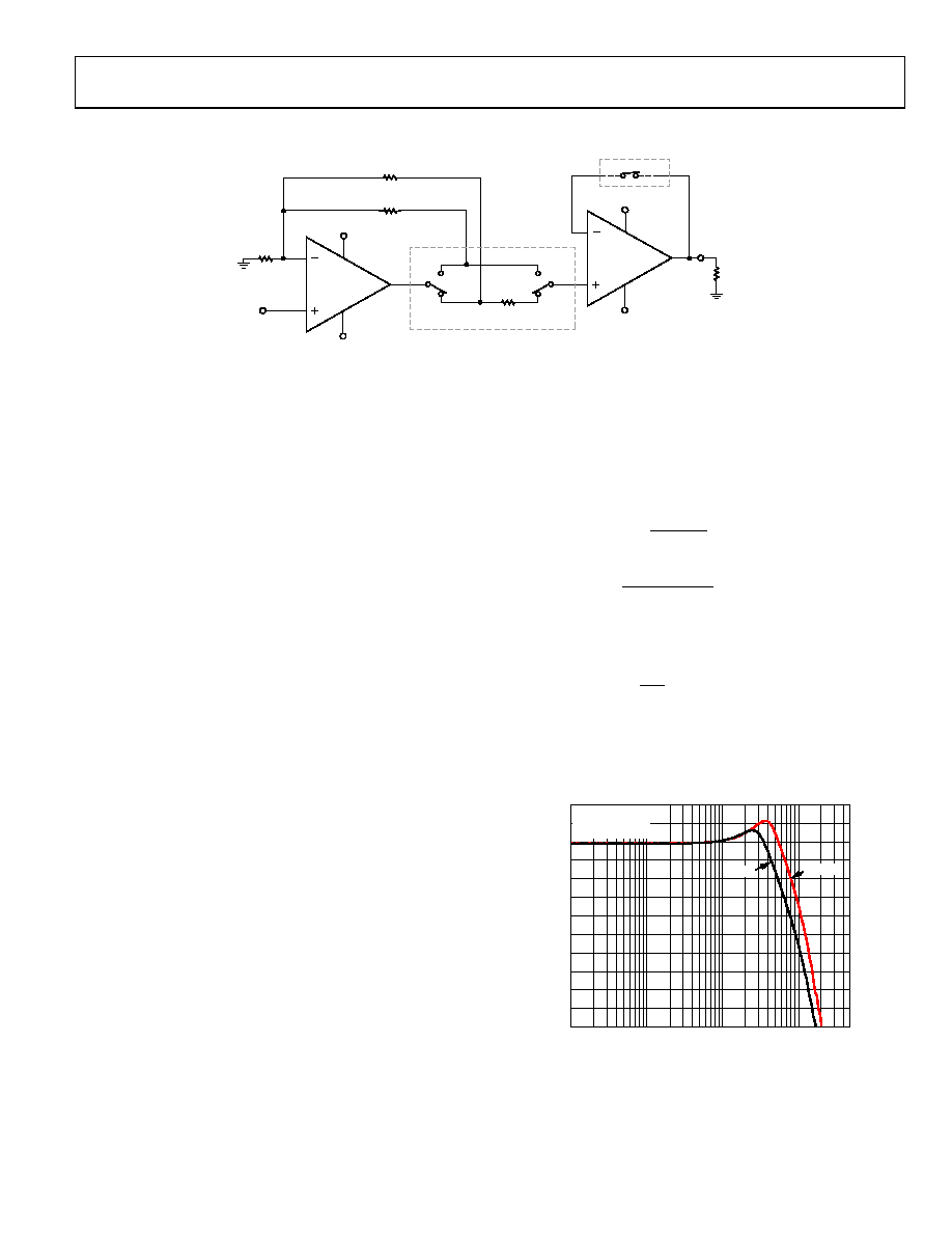
Figure 52. Using the ADA4896-2 and the ADG633 to Construct a Low Noise, Gain Selectable Amplifier to Drive a Low Resistive Load
A gain selectable amplifier makes processing a wide range of
input signals possible. A traditional gain selectable amplifier
uses switches in the feedback loops connecting to the inverting
input. The switch resistances degrade the noise performance of
the amplifier, as well as adding significant capacitance on the
inverting input node. The noise and capacitance issues can be
especially bothersome when working with low noise amplifiers.
Also, the switch resistances contribute to nonlinear gain error,
which is undesirable.
Figure 52 presents an innovative switching technique used in
the gain selectable amplifier such that the 1 nV/Hz noise per-
formance of the ADA4896-2 is preserved while the nonlinear
gain error is much reduced. With this technique, the user can
also choose switches with minimal capacitance to optimize the
bandwidth of the circuit.
In the circuit shown in Figure 52, the switches are implemented
with the ADG633 and are configured such that either S1A and
S2A are on, or S1B and S2B are on. In this example, when the
S1A and S2A switches are on, the first stage amplifier gain is +4.
When the S1B and S2B switches are on, the first stage amplifier
gain is +2. The first set of switches of the ADG633 is placed on
the output side of the feedback loop, and the second set of switches
is used to sample at a point (V1 or V2) where switch resistances
and nonlinear resistances do not matter. In this way, the gain
error can be reduced while preserving the noise performance
of the ADA4896-2.
Note that the input bias current of the output buffer can cause
problems with the impedance of the S2A and S2B sampling
switches. Both sampling switches are not only nonlinear with
voltage but with temperature as well. If this is an issue, place the
unused switch of the ADG633 (S3B) in the feedback path of the
output buffer to balance the bias currents (see Figure 52).
In addition, the bias current of the input amplifier causes
an offset at the output that varies based on the gain setting.
Because the input amplifier and the output buffer are mono-
lithic, the relative matching of their bias currents can be used
to cancel out the varying offset. Placing a resistor equal to the
difference between RF2 and RF1 in series with Switch S2A results
in a more constant offset voltage.
The following derivation shows that sampling at V1 yields the
desired signal gain without gain error. RS denotes the switch
resistance. V2 can be derived using the same method.
+
×
=
G1
S1
F1
IN
01
R
V
1
(7)
+
×
=
S1
G1
F1
G1
F1
01
R
V
V1
(8)
Substituting Equation 1 into Equation 2, the following
derivation is obtained.
+
×
=
G1
F1
IN
R
V
V1
1
(9)
Note that if V01 yields the desired signal gain without gain
error, the buffered output V02 will also be free from gain
error. Figure 53 shows the normalized frequency response of
the circuit at V02.
–30
–27
–24
–21
–18
–15
–12
–9
–6
–3
0
3
6
N
O
R
M
A
L
IZ
E
D
C
L
OS
E
D
-L
OOP
GA
IN
(
d
B
)
FREQUENCY (MHz)
VS = ±5V
VIN = 100mV p-p
RL = 1k
G = +2
G = +4
0.1
1
10
100
500
09
44
7-
0
64
Figure 53. Frequency Response of V02/VIN
B
相关PDF资料 |
PDF描述 |
|---|---|
| 77313-101-20LF | HDR STR DR.100 DP |
| TSW-202-07-G-S | CONN HEADER 2POS .200" SNGL |
| TSW-105-20-T-S | CONN HEADER 5POS .100" SNGL |
| TSM-102-01-T-SH-P-TR | CONN HEADER 2POS .100" SNGL SMD |
| 9-146309-0-32 | CONN HEADR BRKWAY .100 64POS R/A |
相关代理商/技术参数 |
参数描述 |
|---|---|
| ADA4897-2ARMZ-RL | 功能描述:IC OPAMP RR 230MHZ LP 10MSOP RoHS:是 类别:集成电路 (IC) >> Linear - Amplifiers - Instrumentation 系列:- 标准包装:73 系列:Over-The-Top® 放大器类型:通用 电路数:4 输出类型:满摆幅 转换速率:0.07 V/µs 增益带宽积:200kHz -3db带宽:- 电流 - 输入偏压:1nA 电压 - 输入偏移:285µV 电流 - 电源:50µA 电流 - 输出 / 通道:25mA 电压 - 电源,单路/双路(±):2 V ~ 44 V,±1 V ~ 22 V 工作温度:-40°C ~ 85°C 安装类型:表面贴装 封装/外壳:16-WFDFN 裸露焊盘 供应商设备封装:16-DFN-EP(5x3) 包装:管件 |
| ADA4897-2TRMZ-EP | 制造商:Analog Devices 功能描述:LOW NOISE LOW POWER R/R OP AMP DUAL - Rail/Tube 制造商:Analog Devices 功能描述:IC OPAMP GP 230MHZ RRO 10MSOP 制造商:Analog Devices 功能描述:Low Noise Low Power R/R Op Amp Dual |
| ADA4898-1 | 制造商:AD 制造商全称:Analog Devices 功能描述:High Voltage, Low Noise, Low Distortion, Unity Gain Stable, High Speed Op Amp |
| ADA4898-1YRD-EBZ | 制造商:Analog Devices 功能描述:HIGH VOLTAGE, LOW NOISE, LOW DISTORTION, UNITY-GAIN STABLE, - Boxed Product (Development Kits) |
| ADA4898-1YRDZ | 功能描述:IC OPAMP VF ULN ULDIST 8SOIC RoHS:是 类别:集成电路 (IC) >> Linear - Amplifiers - Instrumentation 系列:- 标准包装:2,500 系列:- 放大器类型:通用 电路数:4 输出类型:- 转换速率:0.6 V/µs 增益带宽积:1MHz -3db带宽:- 电流 - 输入偏压:45nA 电压 - 输入偏移:2000µV 电流 - 电源:1.4mA 电流 - 输出 / 通道:40mA 电压 - 电源,单路/双路(±):3 V ~ 32 V,±1.5 V ~ 16 V 工作温度:0°C ~ 70°C 安装类型:表面贴装 封装/外壳:14-TSSOP(0.173",4.40mm 宽) 供应商设备封装:14-TSSOP 包装:带卷 (TR) 其它名称:LM324ADTBR2G-NDLM324ADTBR2GOSTR |
发布紧急采购,3分钟左右您将得到回复。