参数资料
| 型号: | ADA4937-1YCPZ-RL |
| 厂商: | Analog Devices Inc |
| 文件页数: | 29/29页 |
| 文件大小: | 0K |
| 描述: | IC ADC DIFF DRIVER 16-LFCSP |
| 设计资源: | Driving AD9233/46/54 ADCs in AC-Coupled Baseband Appls (CN0051) |
| 标准包装: | 5,000 |
| 类型: | ADC 驱动器 |
| 应用: | 数据采集 |
| 安装类型: | 表面贴装 |
| 封装/外壳: | 16-VFQFN 裸露焊盘,CSP |
| 供应商设备封装: | 16-LFCSP-VQ |
| 包装: | 带卷 (TR) |
第1页第2页第3页第4页第5页第6页第7页第8页第9页第10页第11页第12页第13页第14页第15页第16页第17页第18页第19页第20页第21页第22页第23页第24页第25页第26页第27页第28页当前第29页
ADA4937-1/ADA4937-2
Data Sheet
Rev. D | Page 8 of 28
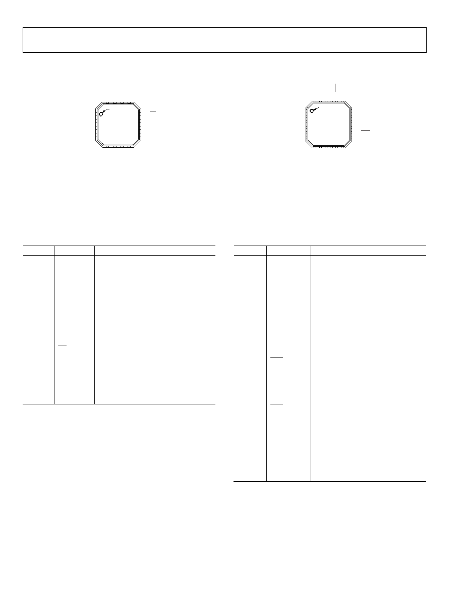
PIN CONFIGURATIONS AND FUNCTION DESCRIPTIONS
NOTES
1. EXPOSED PADDLE. THE EXPOSED PAD IS NOT
ELECTRICALLY CONNECTED TO THE DEVICE. IT IS
TYPICALLY SOLDERED TO GROUND OR A POWER
PLANE ON THE PCB THAT IS THERMALLY CONDUCTIVE.
1
–FB
2
+IN
3
–IN
4
+FB
11 –OUT
12 PD
10 +OUT
9
VOCM
5
+V
S
6
+V
S
7
+V
S
8
+V
S
15
–V
S
16
–V
S
14
–V
S
13
–V
S
ADA4937-1
TOP VIEW
(Not to Scale)
PIN 1
INDICATOR
06591-
005
Figure 5. ADA4937-1 Pin Configuration
06591-
006
PIN 1
INDICATOR
1
2
3
4
5
6
15
16
17
18
14
13
7
8
9
1
12
10
21
22
23
24
+
IN1
20
19
TOP VIEW
(Not to Scale)
ADA4937-2
–IN1
+FB1
+VS1
–FB2
+IN2
–VS2
VOCM1
+OUT1
PD2
–OUT2
–I
N2
+
F
B2
+V
S2
V
O
CM
2
+
OU
T2
+V
S2
–V
S1
–V
S1
–
F
B1
P
D1
–O
UT
1
NOTES
1. EXPOSED PADDLE. THE EXPOSED PAD IS NOT
ELECTRICALLY CONNECTED TO THE DEVICE. IT IS
TYPICALLY SOLDERED TO GROUND OR A POWER
PLANE ON THE PCB THAT IS THERMALLY CONDUCTIVE.
Figure 6. ADA4937-2 Pin Configuration
Table 7. ADA4937-1 Pin Function Descriptions
Pin No.
Mnemonic
Description
1
FB
Negative Output for Feedback
Component Connection.
2
+IN
Positive Input Summing Node.
3
IN
Negative Input Summing Node.
4
+FB
Positive Output for Feedback
Component Connection.
5 to 8
+VS
Positive Supply Voltage.
9
VOCM
Output Common-Mode Voltage.
10
+OUT
Positive Output for Load Connection.
11
OUT
Negative Output for Load Connection.
12
PD
Power-Down Pin.
13 to 16
VS
Negative Supply Voltage.
EP
Exposed Paddle. The exposed pad is not
electrically connected to the device. It is
typically soldered to ground or a power
plane on the PCB that is thermally
conductive.
Table 8. ADA4937-2 Pin Function Descriptions
Pin No.
Mnemonic
Description
1
IN1
Negative Input Summing Node 1.
2
+FB1
Positive Output Feedback Pin 1.
3, 4
+VS1
Positive Supply Voltage 1.
5
FB2
Negative Output Feedback Pin 2.
6
+IN2
Positive Input Summing Node 2.
7
IN2
Negative Input Summing Node 2.
8
+FB2
Positive Output Feedback Pin 2.
9, 10
+VS2
Positive Supply Voltage 2.
11
VOCM2
Output Common-Mode Voltage 2.
12
+OUT2
Positive Output 2.
13
OUT2
Negative Output 2.
14
PD2
Power-Down Pin 2.
15, 16
VS2
Negative Supply Voltage 2.
17
VOCM1
Output Common-Mode Voltage 1.
18
+OUT1
Positive Output 1.
19
OUT1
Negative Output 1.
20
PD1
Power-Down Pin 1.
21, 22
VS1
Negative Supply Voltage 1.
23
FB1
Negative Output Feedback Pin 1.
24
+IN1
Positive Input Summing Node 1.
EP
Exposed Paddle. The exposed pad is
not electrically connected to the
device. It is typically soldered to
ground or a power plane on the PCB
that is thermally conductive.
相关PDF资料 |
PDF描述 |
|---|---|
| VE-24N-IV-F1 | CONVERTER MOD DC/DC 18.5V 150W |
| LTC6404IUD-4#TRPBF | IC AMP/DRIVER DIFF 16-QFN |
| VE-24M-IV-F4 | CONVERTER MOD DC/DC 10V 150W |
| VE-24M-IV-F3 | CONVERTER MOD DC/DC 10V 150W |
| LTC6404IUD-2#TRPBF | IC AMP/DRIVER DIFF 16-QFN |
相关代理商/技术参数 |
参数描述 |
|---|---|
| ADA4937-2YCP-EBZ | 功能描述:BOARD EVAL FOR ADA4937-2YCP RoHS:是 类别:编程器,开发系统 >> 评估板 - 运算放大器 系列:- 产品培训模块:Lead (SnPb) Finish for COTS Obsolescence Mitigation Program 标准包装:1 系列:- |
| ADA4937-2YCPZ-R2 | 制造商:Analog Devices 功能描述:SP AMP DIFF AMP DUAL 5.25V 24LFCSP EP - Tape and Reel 制造商:Analog Devices 功能描述:IC DIFF AMP 1.9GHZ 6000V/ LFCSP-24 制造商:Analog Devices 功能描述:IC, DIFF AMP, 1.9GHZ, 6000V/ uS, LFCSP-24, No. of Amplifiers:2, Input Offset Vol |
| ADA4937-2YCPZ-R7 | 功能描述:IC ADC DRIVER DIFF DUAL 24LFCSP RoHS:是 类别:集成电路 (IC) >> 线性 - 放大器 - 专用 系列:- 产品培训模块:Lead (SnPb) Finish for COTS Obsolescence Mitigation Program 标准包装:60 系列:- 类型:可变增益放大器 应用:CATV 安装类型:表面贴装 封装/外壳:20-WQFN 裸露焊盘 供应商设备封装:20-TQFN-EP(5x5) 包装:托盘 |
| ADA4937-2YCPZ-RL | 功能描述:IC ADC DRIVER DUAL DIFF 24LFCSP RoHS:是 类别:集成电路 (IC) >> 线性 - 放大器 - 专用 系列:- 产品培训模块:Lead (SnPb) Finish for COTS Obsolescence Mitigation Program 标准包装:60 系列:- 类型:可变增益放大器 应用:CATV 安装类型:表面贴装 封装/外壳:20-WQFN 裸露焊盘 供应商设备封装:20-TQFN-EP(5x5) 包装:托盘 |
| ADA4938-1 | 制造商:AD 制造商全称:Analog Devices 功能描述:Ultra-Low Distortion Differential ADC Driver |
发布紧急采购,3分钟左右您将得到回复。