- 您现在的位置:买卖IC网 > PDF目录16955 > ADA4950-1YCP-EBZ (Analog Devices Inc)BOARD EVAL FOR ADA4950-1YCP PDF资料下载
参数资料
| 型号: | ADA4950-1YCP-EBZ |
| 厂商: | Analog Devices Inc |
| 文件页数: | 13/28页 |
| 文件大小: | 0K |
| 描述: | BOARD EVAL FOR ADA4950-1YCP |
| 标准包装: | 1 |
| 每 IC 通道数: | 1 - 单 |
| 放大器类型: | 差分 |
| 板类型: | 裸(未填充) |
| 已供物品: | 板 |
| 已用 IC / 零件: | 16-LFCSP 封装 |
第1页第2页第3页第4页第5页第6页第7页第8页第9页第10页第11页第12页当前第13页第14页第15页第16页第17页第18页第19页第20页第21页第22页第23页第24页第25页第26页第27页第28页
ADA4950-1/ADA4950-2
Data Sheet
Rev. A | Page 20 of 28
Table 12. Differential Input, DC-Coupled
Nominal Linear Gain
RF (Ω)
RG (Ω)
RIN, dm (Ω)
Differential Output Noise Density (nV/√Hz)
1
500
1000
9.25
2
500
250
500
12.9
3
500
250||500
333
16.6
Table 13. Single-Ended, Ground-Referenced Input, DC-Coupled, RS = 50
Nominal Linear Gain
RF (Ω)
RG1 (Ω)
RT (Ω) (Std 1%) RIN, se (Ω)
Differential Output Noise Density (nV/√Hz)
1
500
53.6
667
526
9.07
2
500
250
57.6
375
277
12.2
3
500
250||500 61.9
267
194
15.0
1
RG2 = RG1 + (RS||RT).
Similar to the case of a conventional op amp, the output noise
voltage densities can be estimated by multiplying the input-
referred terms at +INx and INx by the appropriate output
factor, where:
(
)
2
1
N
β
G
+
=
2
is the circuit noise gain.
G1
F1
G1
1
R
β
+
=
and
G2
F2
G2
2
R
β
+
=
are the feedback factors.
When the feedback factors are matched, RF1/RG1 = RF2/RG2,
β1 = β2 = β, and the noise gain becomes
G
F
N
R
β
G
+
=
1
Note that the output noise from VOCM goes to 0 in this case. The
total differential output noise density, vnOD, is the root-sum-
square of the individual output noise terms.
∑
=
8
1
i
2
nOi
nOD
v
Table 12 and Table 13 list the three available gain settings,
associated resistor values, input impedance, and output noise
density for both balanced and unbalanced input configurations.
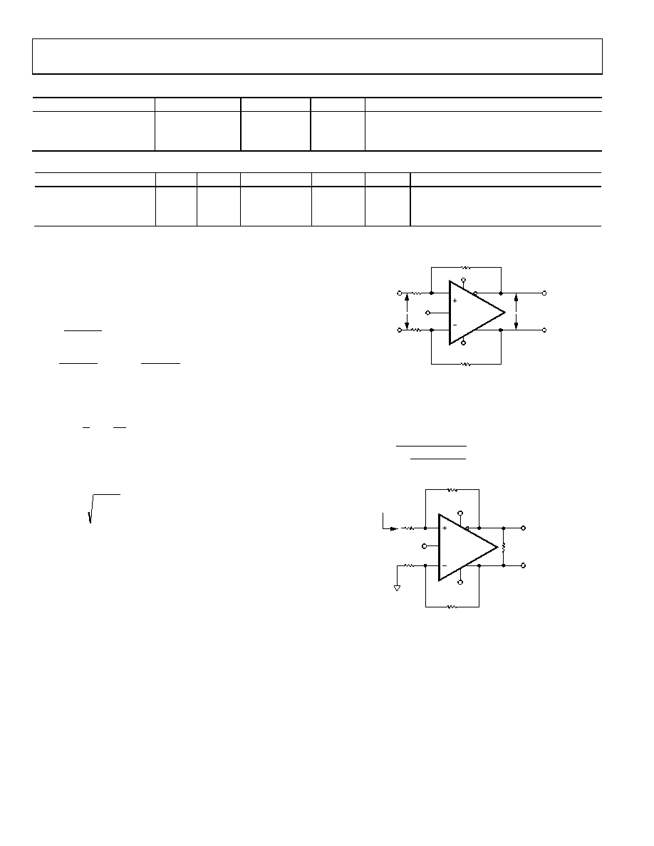
CALCULATING THE INPUT IMPEDANCE FOR AN
APPLICATION CIRCUIT
The effective input impedance of a circuit depends on whether
the amplifier is being driven by a single-ended or differential
signal source. For balanced differential input signals, as shown
RIN, dm = (RG + RG) = 2 × RG
The value of RG depends on the selected gain.
+VS
–VS
+IN
–IN
RF
VOCM
RG
VOUT, dm
VIN, dm
07957-
054
ADA4950-x
Figure 54. ADA4950-x Configured for Balanced (Differential) Inputs
For an unbalanced, single-ended input signal (see Figure 55),
the input impedance is
(
)
+
×
=
F
G
F
G
se
IN
R
2
1
,
ADA4950-x
RL VOUT, dm
+VS
–VS
RG
RF
VOCM
RIN, se
07957-
055
Figure 55. ADA4950-x with Unbalanced (Single-Ended) Input
The input impedance of the circuit is effectively higher than it
is for a conventional op amp connected as an inverter because a
fraction of the differential output voltage appears at the inputs
as a common-mode signal, partially bootstrapping the voltage
across the input resistor, RG. The common-mode voltage at the
amplifier input terminals can be easily determined by noting
that the voltage at the inverting input is equal to the noninverting
output voltage divided down by the voltage divider that is formed
by RF and RG in the lower loop. This voltage is present at both
input terminals due to negative voltage feedback and is in phase
with the input signal, thus reducing the effective voltage across
RG in the upper loop and partially bootstrapping RG.
相关PDF资料 |
PDF描述 |
|---|---|
| LLS2W221MELC | CAP ALUM 220UF 450V 20% SNAP |
| 222D132-4-60/42-0 | BOOT MOLDED |
| ECM18DRKI-S13 | CONN EDGECARD 36POS .156 EXTEND |
| 222D132-3-60/42-0 | BOOT MOLDED |
| 381LX153M025J452 | CAP ALUM 15000UF 25V 20% SNAP |
相关代理商/技术参数 |
参数描述 |
|---|---|
| ADA4950-1YCPZ-R2 | 制造商:Analog Devices 功能描述:SP Amp DIFF AMP Single ±5.5V/11V 16-Pin LFCSP EP T/R 制造商:Analog Devices 功能描述:FIXED GAIN 1,2&3 DIFF ADC DRIVER - Tape and Reel 制造商:Analog Devices 功能描述:SP Amp DIFF AMP Single }5.5V/11V 16-Pin LFCSP EP |
| ADA4950-1YCPZ-R7 | 功能描述:IC AMP DIFF LP 114MA 16LFCSP RoHS:是 类别:集成电路 (IC) >> Linear - Amplifiers - Instrumentation 系列:- 产品培训模块:Differential Circuit Design Techniques for Communication Applications 标准包装:1 系列:- 放大器类型:RF/IF 差分 电路数:1 输出类型:差分 转换速率:9800 V/µs 增益带宽积:- -3db带宽:2.9GHz 电流 - 输入偏压:3µA 电压 - 输入偏移:- 电流 - 电源:40mA 电流 - 输出 / 通道:- 电压 - 电源,单路/双路(±):3 V ~ 3.6 V 工作温度:-40°C ~ 85°C 安装类型:表面贴装 封装/外壳:16-VQFN 裸露焊盘,CSP 供应商设备封装:16-LFCSP-VQ 包装:剪切带 (CT) 产品目录页面:551 (CN2011-ZH PDF) 其它名称:ADL5561ACPZ-R7CT |
| ADA4950-1YCPZ-RL | 功能描述:IC AMP DIFF LP 114MA 16LFCSP RoHS:是 类别:集成电路 (IC) >> Linear - Amplifiers - Instrumentation 系列:- 标准包装:50 系列:- 放大器类型:J-FET 电路数:2 输出类型:- 转换速率:3.5 V/µs 增益带宽积:1MHz -3db带宽:- 电流 - 输入偏压:30pA 电压 - 输入偏移:2000µV 电流 - 电源:200µA 电流 - 输出 / 通道:- 电压 - 电源,单路/双路(±):7 V ~ 36 V,±3.5 V ~ 18 V 工作温度:0°C ~ 70°C 安装类型:通孔 封装/外壳:8-DIP(0.300",7.62mm) 供应商设备封装:8-PDIP 包装:管件 |
| ADA4950-2 | 制造商:AD 制造商全称:Analog Devices 功能描述:Low Power, Selectable Gain Differential ADC Driver, G = 1, 2, 3 |
| ADA4950-2YCP-EBZ | 功能描述:BOARD EVAL FOR ADA4950-2YCP RoHS:是 类别:编程器,开发系统 >> 评估板 - 运算放大器 系列:- 产品培训模块:Lead (SnPb) Finish for COTS Obsolescence Mitigation Program 标准包装:1 系列:- |
发布紧急采购,3分钟左右您将得到回复。