- 您现在的位置:买卖IC网 > PDF目录16955 > ADA4950-1YCP-EBZ (Analog Devices Inc)BOARD EVAL FOR ADA4950-1YCP PDF资料下载
参数资料
| 型号: | ADA4950-1YCP-EBZ |
| 厂商: | Analog Devices Inc |
| 文件页数: | 15/28页 |
| 文件大小: | 0K |
| 描述: | BOARD EVAL FOR ADA4950-1YCP |
| 标准包装: | 1 |
| 每 IC 通道数: | 1 - 单 |
| 放大器类型: | 差分 |
| 板类型: | 裸(未填充) |
| 已供物品: | 板 |
| 已用 IC / 零件: | 16-LFCSP 封装 |
第1页第2页第3页第4页第5页第6页第7页第8页第9页第10页第11页第12页第13页第14页当前第15页第16页第17页第18页第19页第20页第21页第22页第23页第24页第25页第26页第27页第28页
ADA4950-1/ADA4950-2
Data Sheet
Rev. A | Page 22 of 28
INPUT COMMON-MODE VOLTAGE RANGE
The ADA4950-x input common-mode voltage range is shifted
down by approximately one VBE, in contrast to other ADC
drivers with centered input ranges such as the ADA4939-x. The
downward-shifted input common-mode range is especially
suited to dc-coupled, single-ended-to-differential, and single-
supply applications.
For ±5 V operation, the input common-mode voltage range at the
summing nodes of the amplifier is specified as 4.8 V to +3.2 V.
With a 5 V supply, the input common-mode voltage range at the
summing nodes of the amplifier is specified as +0.2 V to +3.2 V.
To avoid nonlinearities, the voltage swing at the +INx and INx
terminals must be confined to these ranges.
INPUT AND OUTPUT CAPACITIVE AC COUPLING
Although the ADA4950-x is well suited to dc-coupled applica-
tions, it is nonetheless possible to use it in ac-coupled circuits.
Input ac coupling capacitors can be inserted between the source
and RG. This ac coupling blocks the flow of the dc common-
mode feedback current and causes the ADA4950-x dc input
common-mode voltage to equal the dc output common-mode
voltage. The ac coupling capacitors must be placed in both
loops to keep the feedback factors matched. Output ac coupling
capacitors can be placed in series between each output and its
respective load.
INPUT SIGNAL SWING CONSIDERATIONS
The input terminals of fully differential amplifiers with external
gain and feedback resistors connect directly to the amplifier
summing nodes; the common-mode voltage swing at these
terminals is generally smaller than the input and output swings.
In most linear applications, the summing node voltages do not
approach levels that result in the forward-biasing of the internal
ESD protection diodes on the amplifier inputs.
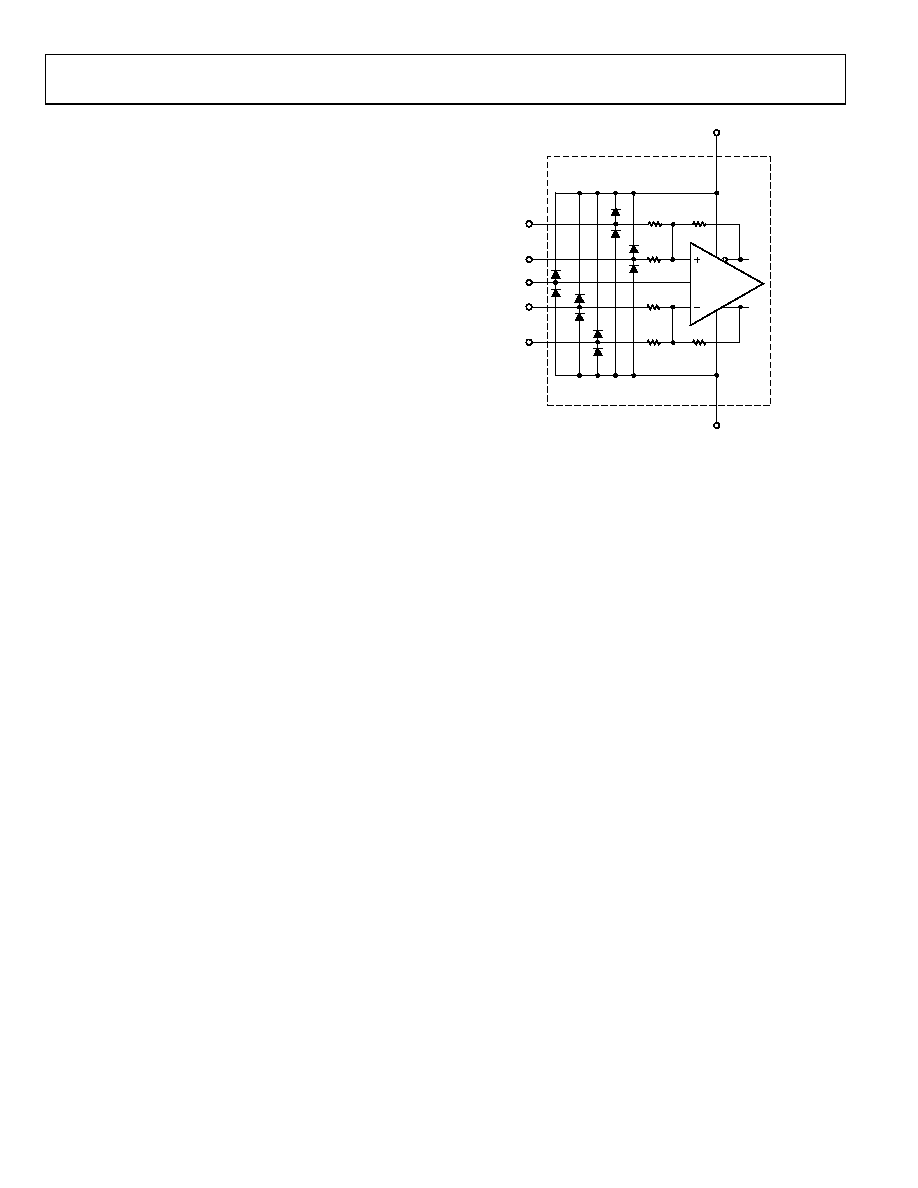
Signals at the inputs of the ADA4950-x are applied to the input
side of the gain resistors, and, if caution is not exercised, these
signals can be large enough to forward-bias the ESD protection
diodes. The four inputs that make up the differential signal paths
each have four ESD diodes in series to the negative supply and
one diode to the positive supply; the VOCM input has one ESD
diode to each supply. Figure 60 illustrates the ESD protection
circuitry.
ADA4950-x
+VS
–VS
500
250
VOCM
250
07
95
7-
2
53
×1
×4
×1
×4
×1
×4
×1
×4
Figure 60. Input ESD Protection Circuitry
SETTING THE OUTPUT COMMON-MODE VOLTAGE
The VOCM pin of the ADA4950-x is internally biased with a vol-
tage divider comprising two 50 kΩ resistors across the supplies,
with a tap at a voltage approximately equal to the midsupply
point, [(+VS) + (VS)]/2. Because of this internal divider, the
VOCM pin sources and sinks current, depending on the externally
applied voltage and its associated source resistance. Relying on
the internal bias results in an output common-mode voltage
that is within approximately 100 mV of the expected value.
In cases where more accurate control of the output common-
mode level is required, it is recommended that an external
source or resistor divider be used with source resistance less
than 100 Ω. If an external voltage divider consisting of equal
resistor values is used to set VOCM to midsupply with greater
accuracy than produced internally, higher values can be used
because the external resistors are placed in parallel with the
section assumes that the VOCM input is driven by a low impedance
voltage source.
It is also possible to connect the VOCM input to a common-mode
level (CML) output of an ADC; however, care must be taken to
ensure that the output has sufficient drive capability. The input
impedance of the VOCM pin is approximately 10 kΩ to a voltage
of nominally midsupply. If multiple ADA4950-x devices share
one ADC reference output, a buffer may be necessary to drive
the parallel inputs.
相关PDF资料 |
PDF描述 |
|---|---|
| LLS2W221MELC | CAP ALUM 220UF 450V 20% SNAP |
| 222D132-4-60/42-0 | BOOT MOLDED |
| ECM18DRKI-S13 | CONN EDGECARD 36POS .156 EXTEND |
| 222D132-3-60/42-0 | BOOT MOLDED |
| 381LX153M025J452 | CAP ALUM 15000UF 25V 20% SNAP |
相关代理商/技术参数 |
参数描述 |
|---|---|
| ADA4950-1YCPZ-R2 | 制造商:Analog Devices 功能描述:SP Amp DIFF AMP Single ±5.5V/11V 16-Pin LFCSP EP T/R 制造商:Analog Devices 功能描述:FIXED GAIN 1,2&3 DIFF ADC DRIVER - Tape and Reel 制造商:Analog Devices 功能描述:SP Amp DIFF AMP Single }5.5V/11V 16-Pin LFCSP EP |
| ADA4950-1YCPZ-R7 | 功能描述:IC AMP DIFF LP 114MA 16LFCSP RoHS:是 类别:集成电路 (IC) >> Linear - Amplifiers - Instrumentation 系列:- 产品培训模块:Differential Circuit Design Techniques for Communication Applications 标准包装:1 系列:- 放大器类型:RF/IF 差分 电路数:1 输出类型:差分 转换速率:9800 V/µs 增益带宽积:- -3db带宽:2.9GHz 电流 - 输入偏压:3µA 电压 - 输入偏移:- 电流 - 电源:40mA 电流 - 输出 / 通道:- 电压 - 电源,单路/双路(±):3 V ~ 3.6 V 工作温度:-40°C ~ 85°C 安装类型:表面贴装 封装/外壳:16-VQFN 裸露焊盘,CSP 供应商设备封装:16-LFCSP-VQ 包装:剪切带 (CT) 产品目录页面:551 (CN2011-ZH PDF) 其它名称:ADL5561ACPZ-R7CT |
| ADA4950-1YCPZ-RL | 功能描述:IC AMP DIFF LP 114MA 16LFCSP RoHS:是 类别:集成电路 (IC) >> Linear - Amplifiers - Instrumentation 系列:- 标准包装:50 系列:- 放大器类型:J-FET 电路数:2 输出类型:- 转换速率:3.5 V/µs 增益带宽积:1MHz -3db带宽:- 电流 - 输入偏压:30pA 电压 - 输入偏移:2000µV 电流 - 电源:200µA 电流 - 输出 / 通道:- 电压 - 电源,单路/双路(±):7 V ~ 36 V,±3.5 V ~ 18 V 工作温度:0°C ~ 70°C 安装类型:通孔 封装/外壳:8-DIP(0.300",7.62mm) 供应商设备封装:8-PDIP 包装:管件 |
| ADA4950-2 | 制造商:AD 制造商全称:Analog Devices 功能描述:Low Power, Selectable Gain Differential ADC Driver, G = 1, 2, 3 |
| ADA4950-2YCP-EBZ | 功能描述:BOARD EVAL FOR ADA4950-2YCP RoHS:是 类别:编程器,开发系统 >> 评估板 - 运算放大器 系列:- 产品培训模块:Lead (SnPb) Finish for COTS Obsolescence Mitigation Program 标准包装:1 系列:- |
发布紧急采购,3分钟左右您将得到回复。