- 您现在的位置:买卖IC网 > PDF目录10027 > ADADC80-12 (Analog Devices Inc)IC ADC 12-BIT INTEGRATED 32-CDIP PDF资料下载
参数资料
| 型号: | ADADC80-12 |
| 厂商: | Analog Devices Inc |
| 文件页数: | 1/16页 |
| 文件大小: | 0K |
| 描述: | IC ADC 12-BIT INTEGRATED 32-CDIP |
| 标准包装: | 1 |
| 位数: | 12 |
| 采样率(每秒): | 40k |
| 数据接口: | 并联 |
| 转换器数目: | 1 |
| 功率耗散(最大): | 800mW |
| 电压电源: | 模拟和数字,双 ± |
| 工作温度: | -25°C ~ 85°C |
| 安装类型: | 通孔 |
| 封装/外壳: | 32-CDIP(0.910",23.12mm) |
| 供应商设备封装: | 32-CDIP 侧面铜焊 |
| 包装: | 管件 |
| 输入数目和类型: | 2 个单端,单极;2 个单端,双极 |
12-Bit Successive-Approximation
Integrated Circuit ADC
ADADC80
Rev.
E
Information furnished by Analog Devices is believed to be accurate and reliable. However, no
responsibilityis assumedbyAnalogDevicesforitsuse,norforanyinfringementsof patentsorother
rightsofthirdpartiesthatmayresultfromitsuse.Specificationssubjecttochangewithoutnotice.No
license is granted by implication or otherwise under any patent or patent rights of Analog Devices.
Trademarksandregisteredtrademarksarethepropertyoftheirrespectiveowners.
One Technology Way, P.O. Box 9106, Norwood, MA 02062-9106, U.S.A.
Tel: 781.329.4700
www.analog.com
Fax: 781.461.3113
2002–2008 Analog Devices, Inc. All rights reserved.
FEATURES
True 12-bit operation: maximum nonlinearity ±0.012%
Low gain temperature coefficient (TC): ±30 ppm/°C
maximum
Low power: 800 mW
Fast conversion time: 25 μs
Precision 6.3 V reference for external application
Short-cycle capability
Parallel data output
Monolithic DAC with scaling resistors for stability
Low chip count, high reliability
Industry-standard pin configuration
“Z” models for ±12 V supplies
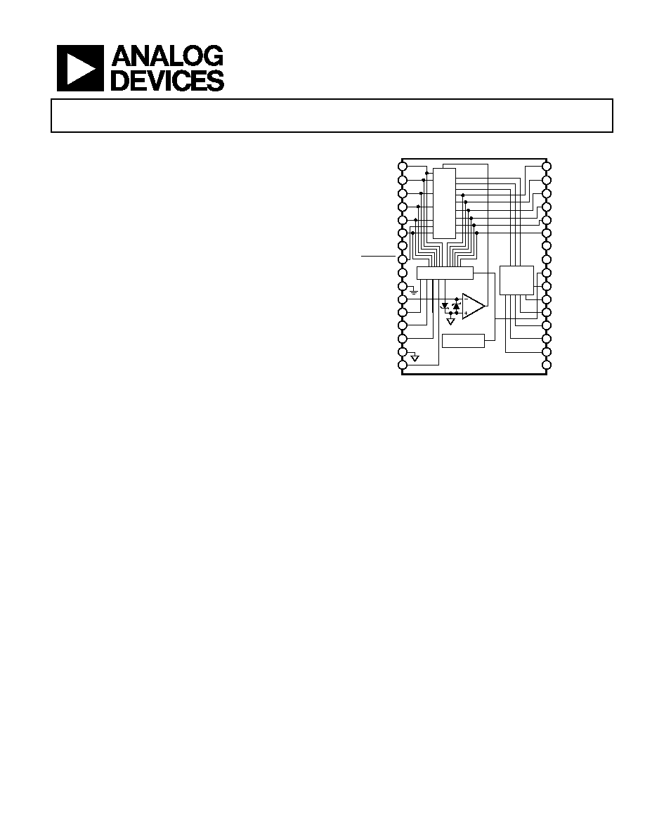
FUNCTIONAL BLOCK DIAGRAM
1
32
2
3
4
5
6
7
8
9
10
11
12
13
14
15
16
31
30
29
28
27
26
25
24
23
22
21
20
19
18
17
BIT 6
BIT 5
BIT 4
BIT 3
BIT 2
BIT 7
BIT 8
BIT 9
BIT 10
BIT 11
BIT 12 (LSB)
BIT 1 (MSB)
DIGITAL GND
10V SPAN IN
20V SPAN IN
ANALOG GND
GAIN ADJUST
NC
5V DIGITAL
SUPPLY
COMPARATOR
IN
BIPOLAR
OFFSET OUT
NC
–15V OR –12V
STATUS
REF OUT (6.3V)
CLOCK OUT
SHORT CYCLE
CLOCK INHIBIT
15V OR 12V
EXTERNAL
CLOCK IN
CONVERT
START
ADADC80
12-BIT
SAR
12-BIT DAC
CLOCK
AND
CONTROL
CIRCUITS
REFERENCE
COMP
NC = NO CONNECT
01
20
2-
001
Figure 1.
PRODUCT DESCRIPTION
The ADADC801 is a complete 12-bit successive-approximation
analog-to-digital converter (ADC) that includes an internal
clock, reference, and comparator. Its hybrid IC design uses MSI
digital and linear monolithic chips in conjunction with a 12-bit
monolithic digital-to-analog converter (DAC) to provide
modular performance and versatility with IC size, price, and
reliability.
Important performance characteristics of the ADADC80
include a maximum linearity error of ±0.012% at 25°C,
maximum gain TC of 30 ppm/°C, typical power dissipation of
800 mW, and maximum conversion time of 25 μs. Monotonic
operation of the feedback DAC guarantees no missing codes
over the temperature range of 25°C to +85°C.
The design of the ADADC80 includes scaling resistors that
provide an analog signal range of ±2.5 V, ±5.0 V, ±10 V, 0 V to
+5.0 V, or 0 V to +10.0 V. The 6.3 V precision reference can be
used for external applications. All digital signals are fully DTL
and TTL compatible; output data is in parallel form.
The ADADC80 is available in grades specified for use over the
25°C to +85°C temperature range and is available in a 32-lead
ceramic DIP.
1 The serial output function is no longer supported on this product after
Date Code 9616.
PRODUCT HIGHLIGHTS
1.
The ADADC80 is a complete 12-bit ADC. No external
components are required to perform a conversion.
2.
A monolithic 12-bit feedback DAC is used for reduced chip
count and higher reliability.
3.
The internal buried Zener reference is laser trimmed to
6.3 V. The reference voltage is available externally and can
supply up to 1.5 mA beyond the current required for the
reference and bipolar offset.
4.
The scaling resistors are included on the monolithic DAC
for exceptional thermal tracking.
5.
The ADADC80 directly replaces other devices of this type,
providing significant increases in performance.
6.
The fast conversion rate of the ADADC80 makes it an
excellent choice for applications requiring high system
throughput rates.
7.
The short cycle and external clock options are provided
for applications requiring faster conversion speed or
lower resolution.
相关PDF资料 |
PDF描述 |
|---|---|
| VE-26J-IX-B1 | CONVERTER MOD DC/DC 36V 75W |
| IDT72245LB15PFI | IC FIFO 1024X18 SYNC 15NS 64QFP |
| VE-21N-MY | CONVERTER MOD DC/DC 18.5V 50W |
| VE-26J-IW-F4 | CONVERTER MOD DC/DC 36V 100W |
| VE-21N-IU-F4 | CONVERTER MOD DC/DC 18.5V 200W |
相关代理商/技术参数 |
参数描述 |
|---|---|
| ADADC80Z10 | 制造商:未知厂家 制造商全称:未知厂家 功能描述:Analog to Digital Converter |
| adadc80-z-10 | 制造商:Rochester Electronics LLC 功能描述:- Bulk 制造商:Analog Devices 功能描述: |
| ADADC80-Z-12 | 功能描述:IC ADC 12BIT INTEGRATED 32-CDIP RoHS:否 类别:集成电路 (IC) >> 数据采集 - 模数转换器 系列:- 产品培训模块:Lead (SnPb) Finish for COTS Obsolescence Mitigation Program 标准包装:250 系列:- 位数:12 采样率(每秒):1.8M 数据接口:并联 转换器数目:1 功率耗散(最大):1.82W 电压电源:模拟和数字 工作温度:-40°C ~ 85°C 安装类型:表面贴装 封装/外壳:48-LQFP 供应商设备封装:48-LQFP(7x7) 包装:管件 输入数目和类型:2 个单端,单极 |
| ADADC80Z-12 | 制造商:AD 制造商全称:Analog Devices 功能描述:Analog-to-Digital Converter, 12-Bit |
| ADADC80Z-CBI-V | 制造商:Rochester Electronics LLC 功能描述:- Bulk 制造商:Analog Devices 功能描述: |
发布紧急采购,3分钟左右您将得到回复。