- 您现在的位置:买卖IC网 > PDF目录10027 > ADADC80-12 (Analog Devices Inc)IC ADC 12-BIT INTEGRATED 32-CDIP PDF资料下载
参数资料
| 型号: | ADADC80-12 |
| 厂商: | Analog Devices Inc |
| 文件页数: | 15/16页 |
| 文件大小: | 0K |
| 描述: | IC ADC 12-BIT INTEGRATED 32-CDIP |
| 标准包装: | 1 |
| 位数: | 12 |
| 采样率(每秒): | 40k |
| 数据接口: | 并联 |
| 转换器数目: | 1 |
| 功率耗散(最大): | 800mW |
| 电压电源: | 模拟和数字,双 ± |
| 工作温度: | -25°C ~ 85°C |
| 安装类型: | 通孔 |
| 封装/外壳: | 32-CDIP(0.910",23.12mm) |
| 供应商设备封装: | 32-CDIP 侧面铜焊 |
| 包装: | 管件 |
| 输入数目和类型: | 2 个单端,单极;2 个单端,双极 |
ADADC80
Rev. E | Page 8 of 16
01
20
2-
00
7
THEORY OF OPERATION
Upon receipt of a CONVERT START command, the ADADC80
converts the voltage at its analog input into an equivalent 12-bit
binary number. This conversion is accomplished as follows:
1.
The 12-bit successive-approximation register (SAR) has its
12-bit outputs connected both to the device bit output pins
and to the corresponding bit inputs of the feedback DAC.
2.
The analog input is successively compared to the feedback
DAC output, one bit at a time (MSB first, LSB last).
3.
The decision to keep or reject each bit is then made at the
completion of each bit comparison period, depending on
the state of the comparator at that time.
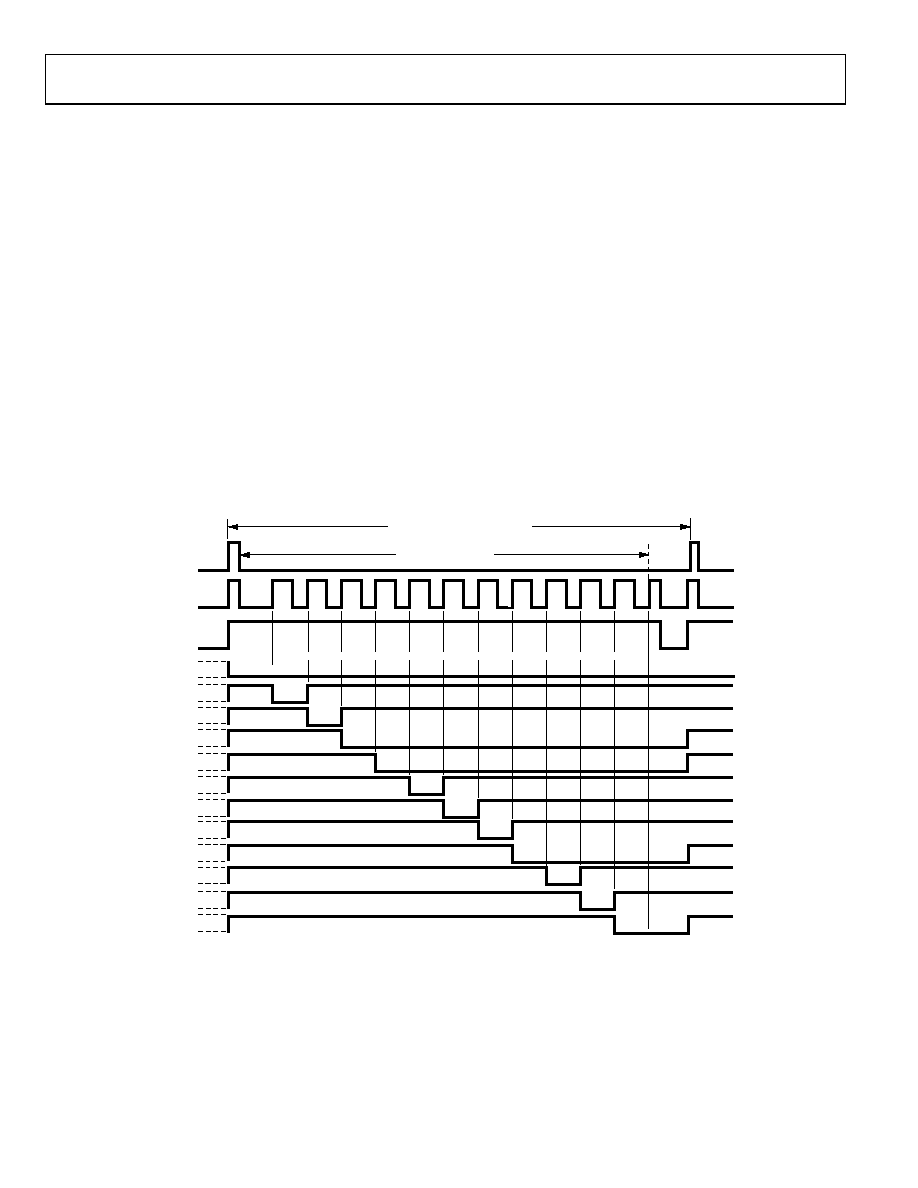
TIMING
The timing diagram is shown in Figure 7. Receipt of a
CONVERT START signal sets the STATUS flag, indicating that
a conversion is in progress. This, in turn, removes the inhibit
applied to the gated clock, permitting it to run through 13 cycles.
All changes to the SAR parallel bit and to the STATUS bit are
initialized on the leading edge, and the gated clock inhibit
signal is removed on the trailing edge of the CONVERT START
signal. At time t0, BIT 1 is reset and BIT 2 to BIT 12 are set
unconditionally. At t1, the BIT 1 decision is made (keep) and
BIT 2 is unconditionally reset. At t2, the BIT 2 decision is made
(keep) and BIT 3 is reset unconditionally. This sequence
continues until the BIT 12 (LSB) decision (keep) is made at t12.
After a 40 ns delay period, the STATUS flag is reset, indicating
that the conversion is complete and the parallel output data is
valid. Resetting the STATUS flag restores the gated clock inhibit
signal, forcing the clock output to the Logic 0 state.
Parallel data bits become valid on the positive-going clock edge
(see Figure 7).
Incorporation of this 40 ns delay guarantees that the parallel
data is valid at the Logic l to Logic 0 transition of the STATUS
flag, permitting a parallel data transfer to be initiated by the
trailing edge of the STATUS signal.
MAXIMUM THROUGHPUT TIME
CONVERT
START1
INTERNAL
CLOCK
STATUS3
MSB
BIT 2
BIT 3
BIT 4
BIT 5
BIT 6
BIT 7
BIT 8
0
1
0
1
0
t0
t2
t1
t4
t3
t6
t5
t8
t7
t10
t9
t12
t11
CONVERSION TIME2
BIT 9
BIT 10
BIT 11
LSB
0
1
0
*
NOTES
1THE CONVERT START PULSE WIDTH IS 100ns MINIMUM AND MUST REMAIN LOW DURING A CONVERSION.
1THE CONVERSION IS INITIATED BY THE RISING EDGE OF THE CONVERT COMMAND.
225s FOR 12 BITS AND 21s FOR 10 BITS (MAXIMUM).
3t1 SHOWS THE MSB DECISION AND t11 SHOWS THE LSB DECISION 40ns PRIOR TO THE STATUS GOING LOW.
*BIT DECISIONS.
Figure 7. Timing Diagram (Binary Code 011001110110)
相关PDF资料 |
PDF描述 |
|---|---|
| VE-26J-IX-B1 | CONVERTER MOD DC/DC 36V 75W |
| IDT72245LB15PFI | IC FIFO 1024X18 SYNC 15NS 64QFP |
| VE-21N-MY | CONVERTER MOD DC/DC 18.5V 50W |
| VE-26J-IW-F4 | CONVERTER MOD DC/DC 36V 100W |
| VE-21N-IU-F4 | CONVERTER MOD DC/DC 18.5V 200W |
相关代理商/技术参数 |
参数描述 |
|---|---|
| ADADC80Z10 | 制造商:未知厂家 制造商全称:未知厂家 功能描述:Analog to Digital Converter |
| adadc80-z-10 | 制造商:Rochester Electronics LLC 功能描述:- Bulk 制造商:Analog Devices 功能描述: |
| ADADC80-Z-12 | 功能描述:IC ADC 12BIT INTEGRATED 32-CDIP RoHS:否 类别:集成电路 (IC) >> 数据采集 - 模数转换器 系列:- 产品培训模块:Lead (SnPb) Finish for COTS Obsolescence Mitigation Program 标准包装:250 系列:- 位数:12 采样率(每秒):1.8M 数据接口:并联 转换器数目:1 功率耗散(最大):1.82W 电压电源:模拟和数字 工作温度:-40°C ~ 85°C 安装类型:表面贴装 封装/外壳:48-LQFP 供应商设备封装:48-LQFP(7x7) 包装:管件 输入数目和类型:2 个单端,单极 |
| ADADC80Z-12 | 制造商:AD 制造商全称:Analog Devices 功能描述:Analog-to-Digital Converter, 12-Bit |
| ADADC80Z-CBI-V | 制造商:Rochester Electronics LLC 功能描述:- Bulk 制造商:Analog Devices 功能描述: |
发布紧急采购,3分钟左右您将得到回复。