- 您现在的位置:买卖IC网 > PDF目录10027 > ADADC80-12 (Analog Devices Inc)IC ADC 12-BIT INTEGRATED 32-CDIP PDF资料下载
参数资料
| 型号: | ADADC80-12 |
| 厂商: | Analog Devices Inc |
| 文件页数: | 4/16页 |
| 文件大小: | 0K |
| 描述: | IC ADC 12-BIT INTEGRATED 32-CDIP |
| 标准包装: | 1 |
| 位数: | 12 |
| 采样率(每秒): | 40k |
| 数据接口: | 并联 |
| 转换器数目: | 1 |
| 功率耗散(最大): | 800mW |
| 电压电源: | 模拟和数字,双 ± |
| 工作温度: | -25°C ~ 85°C |
| 安装类型: | 通孔 |
| 封装/外壳: | 32-CDIP(0.910",23.12mm) |
| 供应商设备封装: | 32-CDIP 侧面铜焊 |
| 包装: | 管件 |
| 输入数目和类型: | 2 个单端,单极;2 个单端,双极 |
ADADC80
Rev. E | Page 12 of 16
Other Ranges
Coding relationships and calibration points for 0 V to +5 V,
2.5 V to +2.5 V, and 5 V to +5 V ranges can be found by
halving the corresponding code equivalents listed for the 0 V to
+10 V and 10 V to +10 V ranges, respectively.
Zero and full-scale calibration can be accomplished to a
precision of approximately ±1/4 LSB using the static adjustment
procedure described previously. By summing a small sine- or
triangular-wave voltage with the signal applied to the analog
input, the output can be cycled through each of the calibration
codes of interest to more accurately determine the center (or
end points) of each discrete quantization level. A detailed
description of this dynamic calibration technique is presented
in A/D Conversion Notes, D. Sheingold, Analog Devices, Inc.,
1977, Part II, Chapter 3.
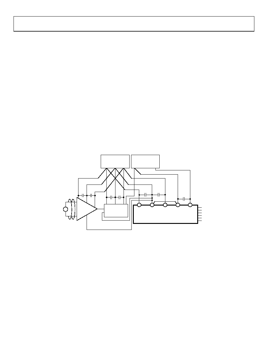
GROUNDING
Many data-acquisition components have two or more ground
pins that are not connected together within the device. These
grounds are usually referred to as the logic power return, analog
common (analog power return), and analog signal ground.
These grounds must be tied together at one point, usually at the
system power-supply ground. Ideally, a single solid ground is
desirable. However, because current flows through the ground
wires and etch stripes of the circuit cards, and because these
paths have resistance and inductance, hundreds of millivolts can
be generated between the system ground point and the ground
pin of the ADADC80. Therefore, separate ground returns
should be provided to minimize the current flow in the path
from sensitive points to the system ground point, and the two
device grounds should be tied together. In this way, supply
currents and logic gate return currents are not summed into the
same return path as analog signals, where they would cause
measurement errors.
Each of the ADADC80 supply terminals should be capacitively
decoupled as close to the ADADC80 as possible. A large value
capacitor, such as 1 μF in parallel with a 0.1 μF capacitor, is
usually sufficient. Analog supplies are bypassed to the analog
power return pin, and the logic supply is bypassed to the logic
power return pin.
17
15
25
10
9
ADADC80
AD583
SAMPLE AND
HOLD
*ANALOG
GROUND
AD521
INST. AMP
OUTPUT
REFERENCE
0.01
F
0.01
F
0.01
F
0.01
F
0.01
F
0.01
F
0.01
F
DIG
COM
5V
C
–15V
C
+15V
ANALOG
PS
DIGITAL
PS
*IF INDEPENDENT, OTHERWISE RETURN
AMPLIFIER REFERENCE TO MECCA AT
ANALOG P.S. COMMON.
0
120
2-
0
15
15V OR
12V
–15V OR
–12V
ANALOG
GND
DIGITAL
GND
5V
DIGITAL
SUPPLY
DIGITAL
GROUND
Figure 15. Basic Grounding Practice
相关PDF资料 |
PDF描述 |
|---|---|
| VE-26J-IX-B1 | CONVERTER MOD DC/DC 36V 75W |
| IDT72245LB15PFI | IC FIFO 1024X18 SYNC 15NS 64QFP |
| VE-21N-MY | CONVERTER MOD DC/DC 18.5V 50W |
| VE-26J-IW-F4 | CONVERTER MOD DC/DC 36V 100W |
| VE-21N-IU-F4 | CONVERTER MOD DC/DC 18.5V 200W |
相关代理商/技术参数 |
参数描述 |
|---|---|
| ADADC80Z10 | 制造商:未知厂家 制造商全称:未知厂家 功能描述:Analog to Digital Converter |
| adadc80-z-10 | 制造商:Rochester Electronics LLC 功能描述:- Bulk 制造商:Analog Devices 功能描述: |
| ADADC80-Z-12 | 功能描述:IC ADC 12BIT INTEGRATED 32-CDIP RoHS:否 类别:集成电路 (IC) >> 数据采集 - 模数转换器 系列:- 产品培训模块:Lead (SnPb) Finish for COTS Obsolescence Mitigation Program 标准包装:250 系列:- 位数:12 采样率(每秒):1.8M 数据接口:并联 转换器数目:1 功率耗散(最大):1.82W 电压电源:模拟和数字 工作温度:-40°C ~ 85°C 安装类型:表面贴装 封装/外壳:48-LQFP 供应商设备封装:48-LQFP(7x7) 包装:管件 输入数目和类型:2 个单端,单极 |
| ADADC80Z-12 | 制造商:AD 制造商全称:Analog Devices 功能描述:Analog-to-Digital Converter, 12-Bit |
| ADADC80Z-CBI-V | 制造商:Rochester Electronics LLC 功能描述:- Bulk 制造商:Analog Devices 功能描述: |
发布紧急采购,3分钟左右您将得到回复。