参数资料
| 型号: | ADAU1361BCPZ-R7 |
| 厂商: | Analog Devices Inc |
| 文件页数: | 32/80页 |
| 文件大小: | 0K |
| 描述: | IC CODEC 24B PLL 32LFCSP |
| 标准包装: | 1,500 |
| 类型: | 音频编解码器 |
| 数据接口: | 串行 |
| 分辨率(位): | 24 b |
| ADC / DAC 数量: | 2 / 2 |
| 三角积分调变: | 无 |
| 电压 - 电源,模拟: | 1.8 V ~ 3.6 V |
| 电压 - 电源,数字: | 1.8 V ~ 3.6 V |
| 工作温度: | -40°C ~ 85°C |
| 安装类型: | 表面贴装 |
| 封装/外壳: | 32-VFQFN 裸露焊盘,CSP |
| 供应商设备封装: | 32-LFCSP-VQ |
| 包装: | 带卷 (TR) |
第1页第2页第3页第4页第5页第6页第7页第8页第9页第10页第11页第12页第13页第14页第15页第16页第17页第18页第19页第20页第21页第22页第23页第24页第25页第26页第27页第28页第29页第30页第31页当前第32页第33页第34页第35页第36页第37页第38页第39页第40页第41页第42页第43页第44页第45页第46页第47页第48页第49页第50页第51页第52页第53页第54页第55页第56页第57页第58页第59页第60页第61页第62页第63页第64页第65页第66页第67页第68页第69页第70页第71页第72页第73页第74页第75页第76页第77页第78页第79页第80页
ADAU1361
Rev. C | Page 38 of 80
CONTROL PORTS
The ADAU1361 can operate in one of two control modes:
I2C control
SPI control
The ADAU1361 has both a 4-wire SPI control port and a
2-wire I2C bus control port. Both ports can be used to set the
registers. The part defaults to I2C mode, but it can be put into
SPI control mode by pulling the CLATCH pin low three times.
The control port is capable of full read/write operation for all
addressable registers. The ADAU1361 must have a valid master
clock in order to write to all registers except for Register R0
(Address 0x4000) and Register R1 (Address 0x4002).
All addresses can be accessed in both a single-address mode
or a burst mode. The first byte (Byte 0) of a control port write
contains the 7-bit chip address plus the R/W bit. The next two
bytes (Byte 1 and Byte 2) together form the subaddress of the
register location within the ADAU1361. This subaddress must
be two bytes long because the memory locations within the
ADAU1361 are directly addressable and their sizes exceed the
range of single-byte addressing. All subsequent bytes (starting
with Byte 3) contain the data. The number of bytes per word
depends on the type of data that is being written.
The control port pins are multifunctional, depending on the
mode in which the part is operating. Table 20 describes these
multiple functions.
Table 20. Control Port Pin Functions
Pin Name
I2C Mode
SPI Mode
SCL/CCLK
SCL: input clock
CCLK: input clock
SDA/COUT
SDA: open-collector
input/output
COUT: output
ADDR1/CDATA
I2C Address Bit 1: input
CDATA: input
ADDR0/CLATCH
I2C Address Bit 0: input
CLATCH: input
BURST MODE WRITING AND READING
Burst mode addressing, where the subaddresses are automatically
incremented at word boundaries, can be used for writing large
amounts of data to contiguous registers. This increment happens
automatically after a single-word write or read unless a stop condi-
tion is encountered (I2C) or CLATCH is brought high (SPI). A
burst write starts like a single-word write, but following the first
data-word, the data-word for the next immediate address can be
written immediately without sending its two-byte address.
The registers in the ADAU1361 are one byte wide with the
exception of the PLL control register, which is six bytes wide.
The autoincrement feature knows the word length at each
subaddress, so the subaddress does not need to be specified
manually for each address in a burst write.
The subaddresses are autoincremented by 1 following each
read or write of a data-word, regardless of whether there is a
valid register word at that address. Address holes in the register
map can be written to or read from without consequence. In
the ADAU1361, these address holes exist at Address 0x4001,
Address 0x4003 to Address 0x4007, Address 0x402E, and
Address 0x4032 to Address 0x4035. A single-byte write to these
registers is ignored by the ADAU1361, and a read returns a
single byte 0x00.
I2C PORT
The ADAU1361 supports a 2-wire serial (I2C-compatible)
microprocessor bus driving multiple peripherals. Two pins,
serial data (SDA) and serial clock (SCL), carry information
between the ADAU1361 and the system I2C master controller.
In I2C mode, the ADAU1361 is always a slave on the bus,
meaning that it cannot initiate a data transfer. Each slave device
is recognized by a unique address. The address and R/W byte
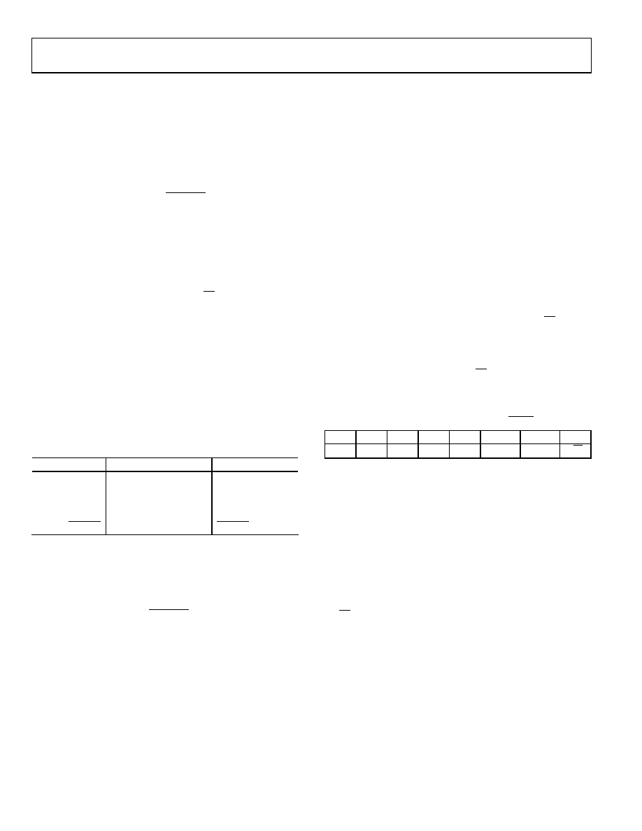
format is shown in
. The address resides in the first
seven bits of the I2C write. Bits[5:6] of the I2C address for the
ADAU1361 are set by the levels on the ADDR1 and ADDR0
pins. The LSB of the address—the R/
W bit—specifies either a
read or write operation. Logic Level 1 corresponds to a read
operation, and Logic Level 0 corresponds to a write operation.
Table 21. ADAU1361 I2C Address and Read/Write Byte Format
Bit 0
Bit 1
Bit 2
Bit 3
Bit 4
Bit 5
Bit 6
Bit 7
0
1
0
ADDR1
ADDR0
R/W
The SDA and SCL pins should each have a 2 kΩ pull-up resistor
on the line connected to it. The voltage on these signal lines
should not be higher than IOVDD (1.8 V to 3.3 V).
Addressing
Initially, each device on the I2C bus is in an idle state and
monitors the SDA and SCL lines for a start condition and
the proper address. The I2C master initiates a data transfer by
establishing a start condition, defined by a high-to-low transition
on SDA while SCL remains high. This indicates that an address/
data stream follows. All devices on the bus respond to the start
condition and shift the next eight bits (the 7-bit address plus the
R/W bit) MSB first. The device that recognizes the transmitted
address responds by pulling the data line low during the ninth
clock pulse. This ninth bit is known as an acknowledge bit. All
other devices withdraw from the bus at this point and return to
the idle condition.
相关PDF资料 |
PDF描述 |
|---|---|
| ADAU1373BCBZ-RL | IC CODEC LP CLASS G HP 81WLCSP |
| ADAU1381BCPZ | IC AUDIO CODEC STEREO LN 32LFCSP |
| ADAU1761BCPZ-RL | IC SIGMADSP CODEC PLL 32LFCSP |
| ADAU1781BCPZ-RL7 | IC SIGMADSP CODEC LN 32LFCSP |
| ADAU1961WBCPZ-R7 | IC STEREO AUD CODEC LP 32LFCSP |
相关代理商/技术参数 |
参数描述 |
|---|---|
| ADAU1361BCPZ-RL | 功能描述:IC CODEC 24B PLL 32LFCSP RoHS:是 类别:集成电路 (IC) >> 接口 - 编解码器 系列:- 标准包装:2,500 系列:- 类型:立体声音频 数据接口:串行 分辨率(位):18 b ADC / DAC 数量:2 / 2 三角积分调变:是 S/N 比,标准 ADC / DAC (db):81.5 / 88 动态范围,标准 ADC / DAC (db):82 / 87.5 电压 - 电源,模拟:2.6 V ~ 3.3 V 电压 - 电源,数字:1.7 V ~ 3.3 V 工作温度:-40°C ~ 85°C 安装类型:表面贴装 封装/外壳:48-WFQFN 裸露焊盘 供应商设备封装:48-TQFN-EP(7x7) 包装:带卷 (TR) |
| ADAU1372BCPZ | 功能描述:General Purpose Interface 24 b I2C, SPI 40-LFCSP-WQ (6x6) 制造商:analog devices inc. 系列:- 包装:托盘 零件状态:有效 类型:通用 数据接口:I2C, SPI 分辨率(位):24 b ADC/DAC 数:4 / 2 三角积分:是 信噪比,ADC/DAC(db)(典型值):- 动态范围,ADC/DAC(db)(典型值):- 电压 - 电源,模拟:1.71 V ~ 3.63 V 电压 - 电源,数字:1.045 V ~ 1.98 V 工作温度:-40°C ~ 85°C 安装类型:表面贴装 封装/外壳:40-WFQFN 裸露焊盘,CSP 供应商器件封装:40-LFCSP-WQ(6x6) 标准包装:1 |
| ADAU1372BCPZRL | 功能描述:IC CODEC LP CLASS G HP 40LFCSP 制造商:analog devices inc. 系列:- 包装:剪切带(CT) 零件状态:Digi-Key 停止供應 类型:通用 数据接口:I2C, SPI 分辨率(位):24 b ADC/DAC 数:4 / 2 三角积分:是 信噪比,ADC/DAC(db)(典型值):- 动态范围,ADC/DAC(db)(典型值):- 电压 - 电源,模拟:1.71 V ~ 3.63 V 电压 - 电源,数字:1.045 V ~ 1.98 V 工作温度:-40°C ~ 85°C 安装类型:表面贴装 封装/外壳:40-WFQFN 裸露焊盘,CSP 供应商器件封装:40-LFCSP-WQ(6x6) 标准包装:1 |
| ADAU1372BCPZ-RL | 功能描述:General Purpose Interface 24 b I2C, SPI 40-LFCSP-WQ (6x6) 制造商:analog devices inc. 系列:- 包装:剪切带(CT) 零件状态:停产 类型:通用 数据接口:I2C, SPI 分辨率(位):24 b ADC/DAC 数:4 / 2 三角积分:是 信噪比,ADC/DAC(db)(典型值):- 动态范围,ADC/DAC(db)(典型值):- 电压 - 电源,模拟:1.71 V ~ 3.63 V 电压 - 电源,数字:1.045 V ~ 1.98 V 工作温度:-40°C ~ 85°C 安装类型:表面贴装 封装/外壳:40-WFQFN 裸露焊盘,CSP 供应商器件封装:40-LFCSP-WQ(6x6) 标准包装:1 |
| ADAU1373BCBZ-R7 | 功能描述:IC CODEC LP W/HDPH AMP 81WLSCP RoHS:是 类别:集成电路 (IC) >> 接口 - 编解码器 系列:- 标准包装:2,500 系列:- 类型:PCM 数据接口:PCM 音频接口 分辨率(位):15 b ADC / DAC 数量:1 / 1 三角积分调变:是 S/N 比,标准 ADC / DAC (db):- 动态范围,标准 ADC / DAC (db):- 电压 - 电源,模拟:2.7 V ~ 3.3 V 电压 - 电源,数字:2.7 V ~ 3.3 V 工作温度:-40°C ~ 85°C 安装类型:表面贴装 封装/外壳:80-VFBGA 供应商设备封装:80-BGA MICROSTAR JUNIOR(5x5) 包装:带卷 (TR) 其它名称:296-21257-2 |
发布紧急采购,3分钟左右您将得到回复。