- 您现在的位置:买卖IC网 > PDF目录10940 > ADAU1381BCBZ-RL (Analog Devices Inc)IC AUDIO CODEC STEREO LN 30WLCSP PDF资料下载
参数资料
| 型号: | ADAU1381BCBZ-RL |
| 厂商: | Analog Devices Inc |
| 文件页数: | 27/84页 |
| 文件大小: | 0K |
| 描述: | IC AUDIO CODEC STEREO LN 30WLCSP |
| 标准包装: | 5,000 |
| 类型: | 立体声音频 |
| 数据接口: | 串行,SPI? |
| 分辨率(位): | 24 b |
| ADC / DAC 数量: | 2 / 2 |
| 三角积分调变: | 无 |
| S/N 比,标准 ADC / DAC (db): | 97 / 100 |
| 动态范围,标准 ADC / DAC (db): | 96.5 / 100 |
| 电压 - 电源,模拟: | 1.8 V ~ 3.65 V |
| 电压 - 电源,数字: | 1.63 V ~ 3.65 V |
| 工作温度: | -25°C ~ 85°C |
| 安装类型: | 表面贴装 |
| 封装/外壳: | 30-UFBGA,WLCSP |
| 供应商设备封装: | 30-WLCSP(3.4x2.64) |
| 包装: | 带卷 (TR) |
| 配用: | EVAL-ADAU1381Z-ND - BOARD EVALUATION FOR ADAU1381 |
第1页第2页第3页第4页第5页第6页第7页第8页第9页第10页第11页第12页第13页第14页第15页第16页第17页第18页第19页第20页第21页第22页第23页第24页第25页第26页当前第27页第28页第29页第30页第31页第32页第33页第34页第35页第36页第37页第38页第39页第40页第41页第42页第43页第44页第45页第46页第47页第48页第49页第50页第51页第52页第53页第54页第55页第56页第57页第58页第59页第60页第61页第62页第63页第64页第65页第66页第67页第68页第69页第70页第71页第72页第73页第74页第75页第76页第77页第78页第79页第80页第81页第82页第83页第84页
ADAU1381
Rev. B | Page 33 of 84
CONTROL PORTS
The ADAU1381 can operate in one of two control modes: I2C
control or SPI control.
The ADAU1381 has both a 4-wire SPI control port and a 2-wire
I2C bus control port. Each can be used to set the registers. The
part defaults to I2C mode but can be put into SPI control mode
by pulling the CLATCH pin low three times.
The control port is capable of full read/write operation for all
addressable registers. Most sound engine processing parameters
are controlled by writing new values to the sound engine parameter
register using the control port. Other functions, such as mute,
input/output mode control, and analog signal paths, can be
programmed by writing to the appropriate registers.
All addresses can be accessed in either a single-address mode or
a burst mode. The first byte (Byte 0) of a control port write contains
the 7-bit chip address plus the R/W bit. The next two bytes (Byte 1
and Byte 2) together form the subaddress of the register location
within the ADAU1381. All subsequent bytes (starting with Byte 3)
contain the data, such as control port data, register data, or sound
engine parameter data. The number of bytes per word depends
on the type of data that is being written. The exact formats for
specific types of writes and reads are shown in
to
.
The ADAU1381 has several mechanisms for updating sound
engine parameters in real time without causing pops or clicks.
The control port pins are multifunctional, depending on the
mode in which the part is operating. Table 20 details these
multiple functions.
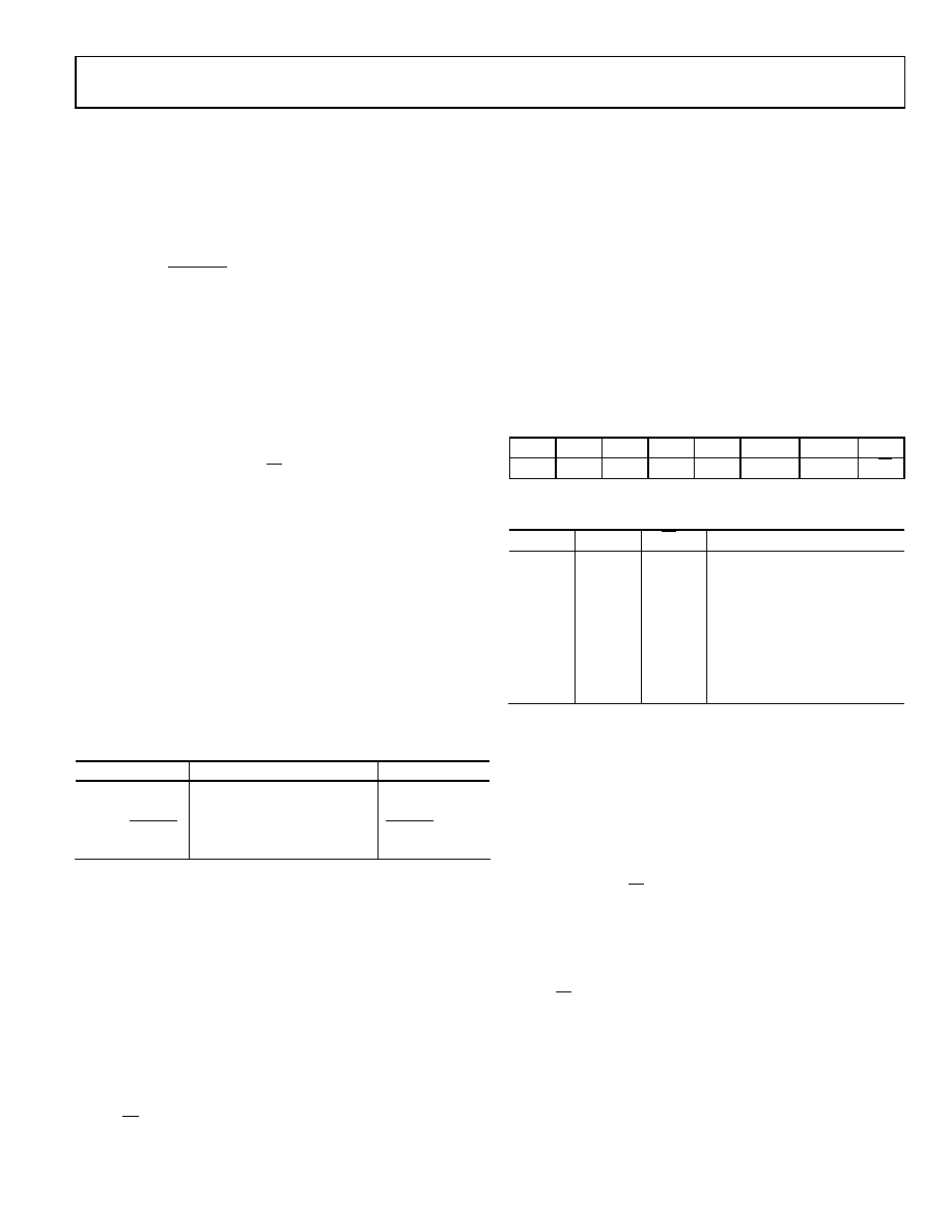
Table 20. Control Port Pin Functions
Pin
I2C Mode
SPI Mode
SCL/CCLK
SCL—input
CCLK—input
SDA/COUT
SDA—open-collector output
COUT—output
ADDR1/CLATCH
I2C Address Bit 1—input
CLATCH—input
ADDR0/CDATA
I2C Address Bit 0—input
CDATA—input
I2C PORT
The ADAU1381 supports a 2-wire serial (I2C-compatible)
microprocessor bus driving multiple peripherals. Two pins,
serial data (SDA) and serial clock (SCL), carry information
between the ADAU1381 and the system I2C master controller.
In I2C mode, the ADAU1381 is always a slave on the bus, meaning
it cannot initiate a data transfer. Each slave device is recognized by
a unique address. The address byte format is shown in Table 21.
The address resides in the first seven bits of the I2C write. The
LSB of this byte sets either a read or write operation. Logic 1
corresponds to a read operation, and Logic 0 corresponds to a
write operation. The full byte addresses, including the pin settings
and R/W bit, are shown in
.
Burst mode addressing, where the subaddresses are automati-
cally incremented at word boundaries, can be used for writing
large amounts of data to contiguous memory locations. This
increment happens automatically after a single-word write unless a
stop condition is encountered. The registers in the ADAU1381
range in width from one to six bytes; therefore, the auto-increment
feature knows the mapping between subaddresses and the word
length of the destination register. A data transfer is always
terminated by a stop condition.
Both SDA and SCL should have 2.0 kΩ pull-up resistors on the
lines connected to them. The voltage on these signal lines should
not be more than AVDD1.
Table 21. I2C Address Byte Format
Bit 0
Bit 1
Bit 2
Bit 3
Bit 4
Bit 5
Bit 6
Bit 7
0
1
0
ADDR1
ADDR0
R/W
Table 22. I2C Addresses
ADDR1
ADDR0
R/W
Slave Address
0
0x70
0
1
0x71
0
1
0
0x72
0
1
0x73
1
0
0x74
1
0
1
0x75
1
0
0x76
1
0x77
Addressing
Initially, each device on the I2C bus is in an idle state and
monitoring the SDA and SCL lines for a start condition and
the proper address. The I2C master initiates a data transfer by
establishing a start condition, defined by a high-to-low transition
on SDA while SCL remains high. This indicates that an address or
an address and data stream follow. All devices on the bus respond
to the start condition and shift the next eight bits (the 7-bit
address plus the R/W bit), MSB first. The device that recognizes
the transmitted address responds by pulling the data line low
during the ninth clock pulse. This ninth bit is known as an
acknowledge bit. All other devices withdraw from the bus at
this point and return to the idle condition.
The R/W bit determines the direction of the data. A Logic 0 on the
LSB of the first byte means the master writes information to the
peripheral, whereas a Logic 1 means the master reads information
from the peripheral after writing the subaddress and repeating
the start address. A data transfer takes place until a stop condition
is encountered. A stop condition occurs when SDA transitions
from low to high while SCL is held high.
shows the
timing of an I2C write, and
shows an I2C read.
相关PDF资料 |
PDF描述 |
|---|---|
| VI-B3K-IW-B1 | CONVERTER MOD DC/DC 40V 100W |
| VI-B3H-IW-B1 | CONVERTER MOD DC/DC 52V 100W |
| VI-B3B-IW-B1 | CONVERTER MOD DC/DC 95V 100W |
| VE-J3B-IX-S | CONVERTER MOD DC/DC 95V 75W |
| VI-B34-IX-B1 | CONVERTER MOD DC/DC 48V 75W |
相关代理商/技术参数 |
参数描述 |
|---|---|
| ADAU1381BCBZ-RL7 | 功能描述:IC AUDIO CODEC STEREO LN 30WLCSP RoHS:是 类别:集成电路 (IC) >> 接口 - 编解码器 系列:- 标准包装:2,500 系列:- 类型:立体声音频 数据接口:串行 分辨率(位):18 b ADC / DAC 数量:2 / 2 三角积分调变:是 S/N 比,标准 ADC / DAC (db):81.5 / 88 动态范围,标准 ADC / DAC (db):82 / 87.5 电压 - 电源,模拟:2.6 V ~ 3.3 V 电压 - 电源,数字:1.7 V ~ 3.3 V 工作温度:-40°C ~ 85°C 安装类型:表面贴装 封装/外壳:48-WFQFN 裸露焊盘 供应商设备封装:48-TQFN-EP(7x7) 包装:带卷 (TR) |
| ADAU1381BCPZ | 功能描述:IC AUDIO CODEC STEREO LN 32LFCSP RoHS:是 类别:集成电路 (IC) >> 接口 - 编解码器 系列:- 标准包装:2,500 系列:- 类型:立体声音频 数据接口:串行 分辨率(位):18 b ADC / DAC 数量:2 / 2 三角积分调变:是 S/N 比,标准 ADC / DAC (db):81.5 / 88 动态范围,标准 ADC / DAC (db):82 / 87.5 电压 - 电源,模拟:2.6 V ~ 3.3 V 电压 - 电源,数字:1.7 V ~ 3.3 V 工作温度:-40°C ~ 85°C 安装类型:表面贴装 封装/外壳:48-WFQFN 裸露焊盘 供应商设备封装:48-TQFN-EP(7x7) 包装:带卷 (TR) |
| ADAU1381BCPZ-RL | 功能描述:IC AUDIO CODEC STEREO LN 32LFCSP RoHS:是 类别:集成电路 (IC) >> 接口 - 编解码器 系列:- 标准包装:2,500 系列:- 类型:立体声音频 数据接口:串行 分辨率(位):18 b ADC / DAC 数量:2 / 2 三角积分调变:是 S/N 比,标准 ADC / DAC (db):81.5 / 88 动态范围,标准 ADC / DAC (db):82 / 87.5 电压 - 电源,模拟:2.6 V ~ 3.3 V 电压 - 电源,数字:1.7 V ~ 3.3 V 工作温度:-40°C ~ 85°C 安装类型:表面贴装 封装/外壳:48-WFQFN 裸露焊盘 供应商设备封装:48-TQFN-EP(7x7) 包装:带卷 (TR) |
| ADAU1381BCPZ-RL7 | 功能描述:IC AUDIO CODEC STEREO LN 32LFCSP RoHS:是 类别:集成电路 (IC) >> 接口 - 编解码器 系列:- 标准包装:2,500 系列:- 类型:立体声音频 数据接口:串行 分辨率(位):18 b ADC / DAC 数量:2 / 2 三角积分调变:是 S/N 比,标准 ADC / DAC (db):81.5 / 88 动态范围,标准 ADC / DAC (db):82 / 87.5 电压 - 电源,模拟:2.6 V ~ 3.3 V 电压 - 电源,数字:1.7 V ~ 3.3 V 工作温度:-40°C ~ 85°C 安装类型:表面贴装 封装/外壳:48-WFQFN 裸露焊盘 供应商设备封装:48-TQFN-EP(7x7) 包装:带卷 (TR) |
| ADAU1382BCPZ | 制造商:Analog Devices 功能描述:STEREO AUDIO CODEC FOR DIG STILL CAM - Trays 制造商:Analog Devices 功能描述:IC AUDIO CODEC 24BIT 96KHZ LFCSP-32 制造商:Analog Devices 功能描述:IC, AUDIO CODEC, 24BIT, 96KHZ, LFCSP-32, Audio CODEC Type:Stereo, No. of ADCs:2, 制造商:Analog Devices 功能描述:AUDIO CODEC |
发布紧急采购,3分钟左右您将得到回复。