- 您现在的位置:买卖IC网 > PDF目录10938 > ADAV803ASTZ-REEL (Analog Devices Inc)IC CODEC AUDIO R-DVD 3.3V 64LQFP PDF资料下载
参数资料
| 型号: | ADAV803ASTZ-REEL |
| 厂商: | Analog Devices Inc |
| 文件页数: | 7/60页 |
| 文件大小: | 0K |
| 描述: | IC CODEC AUDIO R-DVD 3.3V 64LQFP |
| 标准包装: | 1,500 |
| 类型: | 音频编解码器 |
| 数据接口: | 串行 |
| 分辨率(位): | 24 b |
| ADC / DAC 数量: | 2 / 2 |
| 三角积分调变: | 无 |
| 动态范围,标准 ADC / DAC (db): | 102 / 101 |
| 电压 - 电源,模拟: | 3 V ~ 3.6 V |
| 电压 - 电源,数字: | 3 V ~ 3.6 V |
| 工作温度: | -40°C ~ 85°C |
| 安装类型: | 表面贴装 |
| 封装/外壳: | 64-LQFP |
| 供应商设备封装: | 64-LQFP(10x10) |
| 包装: | 带卷 (TR) |
| 配用: | EVAL-ADAV803EBZ-ND - BOARD EVALUATION FOR ADAV803 |
第1页第2页第3页第4页第5页第6页当前第7页第8页第9页第10页第11页第12页第13页第14页第15页第16页第17页第18页第19页第20页第21页第22页第23页第24页第25页第26页第27页第28页第29页第30页第31页第32页第33页第34页第35页第36页第37页第38页第39页第40页第41页第42页第43页第44页第45页第46页第47页第48页第49页第50页第51页第52页第53页第54页第55页第56页第57页第58页第59页第60页
ADAV803
Rev. A | Page 15 of 60
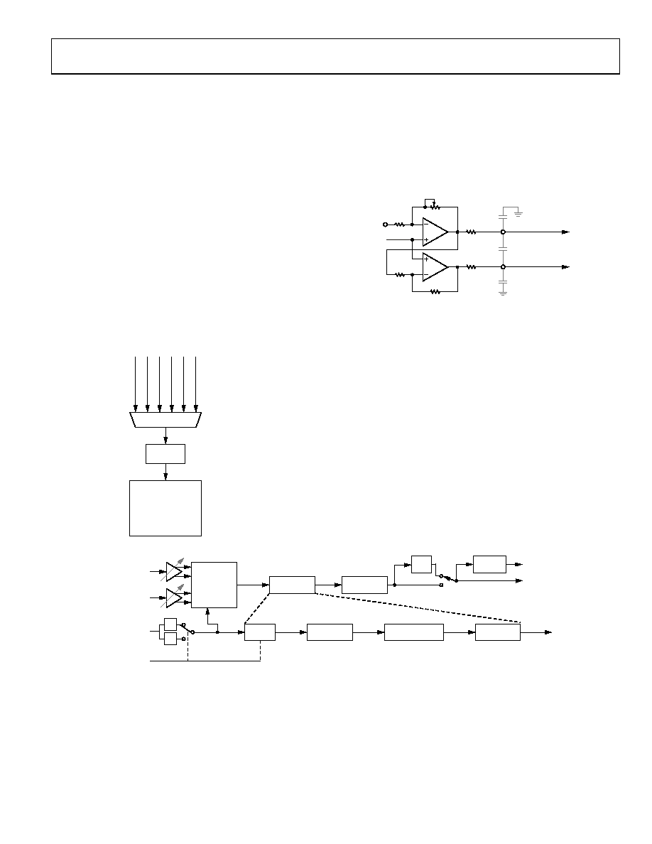
FUNCTIONAL DESCRIPTION
ADC SECTION
The ADAV803’s ADC section is implemented using a second-
order multibit (5 bits) Σ-Δ modulator. The modulator is
sampled at either half of the ADC MCLK rate (modulator clock
= 128 × fS) or one-quarter of the ADC MCLK rate (modulator
clock = 64 × fS). The digital decimator consists of a Sinc^5 filter
followed by a cascade of three half-band FIR filters. The Sinc
decimates by a factor of 16 at 48 kHz and by a factor of 8 at
96 kHz. Each of the half-band filters decimates by a factor of 2.
Figure 23 shows the details of the ADC section. By default, the
ADC assumes that the MCLK rate is 256 times the sample rate.
The ADC can be clocked by a number of different clock sources
to control the sample rate. MCLK selection for the ADC is set
by Internal Clocking Control Register 1 (Address 0x76). The
ADC provides an output word of up to 24 bits of resolution in
twos complement format. The output word can be routed to the
output ports, the sample rate converter, or the S/PDIF digital
transmitter.
P
L
2I
NT
E
RNAL
P
L
1I
NT
E
RNAL
MC
L
K
I
XI
N
REG 0x76
BITS[4:2]
REG 0x6F
BITS[1:0]
DI
R
P
L
(256
×
f
S
)
04
75
6-
02
3
DI
R
P
L
(512
×
f
S
)
ADC MCLK
DIVIDER
ADC
MCLK
ADC
Figure 23. Clock Path Control on the ADC
Programmable Gain Amplifier (PGA)
The input of the record channel features a PGA that converts
the single-ended signal to a differential signal, which is applied
to the analog Σ-Δ modulator of the ADC. The PGA can be
programmed to amplify a signal by up to 24 dB in 0.5 dB
increments. Figure 24 shows the structure of the PGA circuit.
4k TO 64k
125
TO
MODULATOR
CAPxN
CAPxP
EXTERNAL
CAPACITOR
(1nF NPO)
EXTERNAL
CAPACITOR
(1nF NPO)
EXTERNAL
CAPACITOR
(1nF NPO)
8k
VREF
04
756
-02
4
4k
125
Figure 24. PGA Block Diagram
Analog Σ-Δ Modulator
The ADC features a second-order, multibit, Σ-Δ modulator. The
input features two integrators in cascade followed by a flash
converter. This multibit output is directed to a scrambler,
followed by a DAC for loop feedback. The flash ADC output is
also converted from thermometer coding to binary coding for
input as a 5-bit word to the decimator. Figure 25 shows the
ADC block diagram.
The ADC also features independent digital volume control for
the left and right channels. The volume control consists of
256 linear steps, with each step reducing the digital output
codes by 0.39%. Each channel also has a peak detector that
records the peak level of the input signal. The peak detector
register is cleared by reading it.
0
475
6-
02
5
ADC MCLK
AMC
(REG 0x6E
BIT 7)
MULTIBIT
Σ-Δ
MODULATOR
DECIMATOR
HPF
PEAK
DETECT
VOLUME
CONTROL
SINC^5
HALF-BAND
FILTER
MODULATOR
CLOCK
(6.144MHz MAX)
384kHz
768kHz
SINC
COMPENSATION
192kHz
384kHz
HALF-BAND
FILTER
96kHz
192kHz
48kHz
96kHz
÷2
÷4
Figure 25. ADC Block Diagram
相关PDF资料 |
PDF描述 |
|---|---|
| AD1939YSTZRL | IC CODEC 24BIT ADC/DAC 64-LQFP |
| AD1937WBSTZ-RL | IC CODEC 4/ADC DIFF OUT 64-LQFP |
| AD1938WBSTZ-RL | IC CODEC 24BIT 4ADC/8DAC 48LQFP |
| AD1938YSTZRL | IC CODEC 24BIT 4ADC/8DAC 48LQFP |
| MCF5213LCVM80 | IC MCU 256K FLASH 80MHZ 81MAPBGA |
相关代理商/技术参数 |
参数描述 |
|---|---|
| ADAV804AST | 制造商:Analog Devices 功能描述:AUDIO CODEC FOR RECORDABLE DVD - Bulk |
| ADAV804ASTZ | 制造商:Analog Devices 功能描述: |
| ADB.1X40 | 制造商:FACOM 功能描述:SCREWDRIVER STUB POZI NO.1 制造商:FACOM 功能描述:SCREWDRIVER, STUB, POZI NO.1 制造商:FACOM 功能描述:SCREWDRIVER, STUB, POZI NO.1; Overall Length:90mm; Blade Length:40mm; SVHC:No SVHC (19-Dec-2012); Range:PZ1; Screwdriver Type:Pozi; Tip / Nozzle Size:PZ1; Tip / Nozzle Style:Pozidriv ;RoHS Compliant: NA |
| ADB0039 | 制造商:AVOCENT 功能描述:Cyclades - Crossover adapter - RJ-45 (M) - RJ-45 (F) |
| ADB-1 | 制造商:IDEC CORPORATION 功能描述:LACHING BEAM ATTACH |
发布紧急采购,3分钟左右您将得到回复。