- 您现在的位置:买卖IC网 > PDF目录378277 > ADC0802LCN (INTERSIL CORP) 8-Bit, Microprocessor- Compatible, A/D Converters PDF资料下载
参数资料
| 型号: | ADC0802LCN |
| 厂商: | INTERSIL CORP |
| 元件分类: | ADC |
| 英文描述: | 8-Bit, Microprocessor- Compatible, A/D Converters |
| 中文描述: | 1-CH 8-BIT SUCCESSIVE APPROXIMATION ADC, PARALLEL ACCESS, CDIP20 |
| 封装: | CERDIP-20 |
| 文件页数: | 21/41页 |
| 文件大小: | 1118K |
| 代理商: | ADC0802LCN |
第1页第2页第3页第4页第5页第6页第7页第8页第9页第10页第11页第12页第13页第14页第15页第16页第17页第18页第19页第20页当前第21页第22页第23页第24页第25页第26页第27页第28页第29页第30页第31页第32页第33页第34页第35页第36页第37页第38页第39页第40页第41页
Functional Description
(Continued)
100
capacitor— both the R and C are placed outside the feed-
back loop— from the output of an op amp, if used.
series
resistor
can
be
used
to
isolate
this
2.3.4 Noise
The leads to the analog inputs (pins 6 and 7) should be kept
as short as possible to minimize input noise coupling. Both
noise and undesired digital clock coupling to these inputs
can cause system errors. The source resistance for these in-
puts should, in general, be kept below 5 k
. Larger values of
source resistance can cause undesired system noise
pickup. Input bypass capacitors, placed from the analog in-
puts to ground, will eliminate system noise pickup but can
create analog scale errors as these capacitors will average
the transient input switching currents of the A/D (see section
2.3.1.). This scale error depends on both a large source re-
sistance and the use of an input bypass capacitor. This error
can be eliminated by doing a full-scale adjustment of the A/D
(adjust V
/2 for a proper full-scale reading— see section
2.5.2 on Full-Scale Adjustment) with the source resistance
and input bypass capacitor in place.
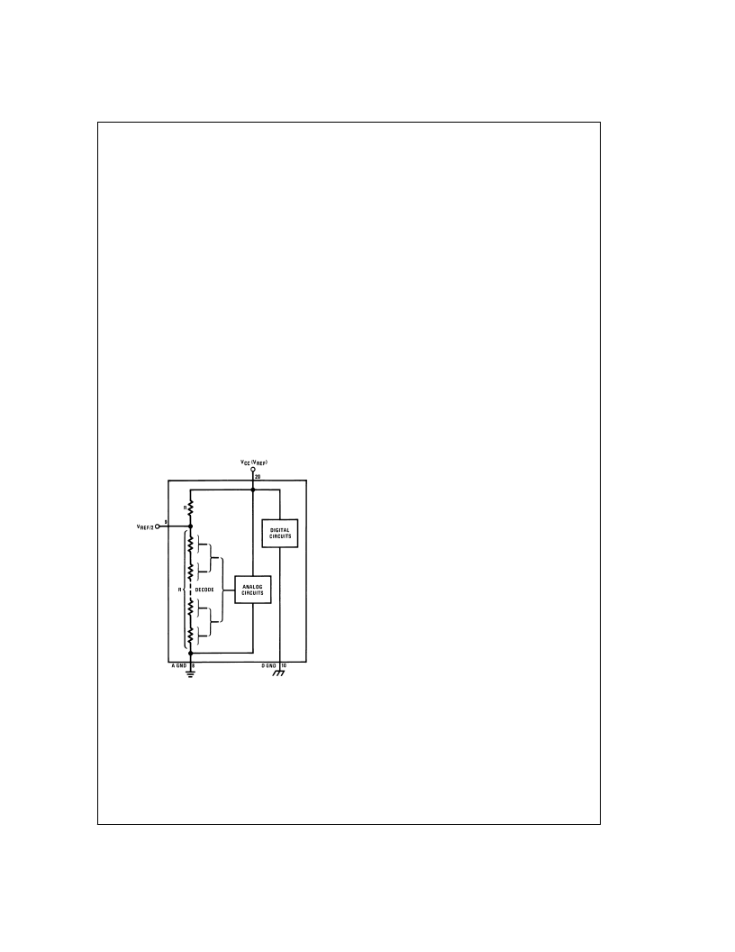
2.4 Reference Voltage
2.4.1 Span Adjust
For maximum applications flexibility, these A/Ds have been
designed to accommodate a 5 V
, 2.5 V
or an adjusted
voltage reference. This has been achieved in the design of
the IC as shown in Figure 6
Notice that the reference voltage for the IC is either
1
2
of the
voltage applied to the V
supply pin, or is equal to the volt-
age that is externally forced at the V
/2 pin. This allows for
a ratiometric voltage reference using the V
CC
supply, a 5
V
reference voltage can be used for the V
supply or a
voltage less than 2.5 V
can be applied to the V
/2 input
for increased application flexibility. The internal gain to the
V
/2 input is 2, making the full-scale differential input volt-
age twice the voltage at pin 9.
An example of the use of an adjusted reference voltage is to
accommodate a reduced span— or dynamic voltage range
of the analog input voltage. If the analog input voltage were
to range from 0.5 V
to 3.5 V
, instead of 0V to 5 V
DC
, the
span would be 3V as shown in Figure 7 With 0.5 V
ap-
plied to the V
() pin to absorb the offset, the reference volt-
age can be made equal to
1
2
of the 3V span or 1.5 V
. The
A/D now will encode the V
(+) signal from 0.5V to 3.5 V with
the 0.5V input corresponding to zero and the 3.5 V
input
corresponding to full-scale. The full 8 bits of resolution are
therefore applied over this reduced analog input voltage
range.
2.4.2 Reference Accuracy Requirements
The converter can be operated in a ratiometric mode or an
absolute mode. In ratiometric converter applications, the
magnitude of the reference voltage is a factor in both the out-
put of the source transducer and the output of the A/D con-
verter and therefore cancels out in the final digital output
code. The ADC0805 is specified particularly for use in ratio-
metric applications with no adjustments required. In absolute
conversion applications, both the initial value and the tem-
perature stability of the reference voltage are important fac-
tors in the accuracy of the A/D converter. For V
/2 volt-
ages of 2.4 V
nominal value, initial errors of
±
10 mV
will
cause conversion errors of
±
1 LSB due to the gain of 2 of the
V
/2 input. In reduced span applications, the initial value
and the stability of the V
/2 input voltage become even
more important. For example, if the span is reduced to 2.5V,
the analog input LSB voltage value is correspondingly re-
duced from 20 mV (5V span) to 10 mV and 1 LSB at the
V
/2 input becomes 5 mV. As can be seen, this reduces
the allowed initial tolerance of the reference voltage and re-
quires correspondingly less absolute change with tempera-
ture variations. Note that spans smaller than 2.5V place
even tighter requirements on the initial accuracy and stability
of the reference source.
In general, the magnitude of the reference voltage will re-
quire an initial adjustment. Errors due to an improper value
of reference voltage appear as full-scale errors in the A/D
transfer function. IC voltage regulators may be used for ref-
erences if the ambient temperature changes are not exces-
sive. The LM336B 2.5V IC reference diode (from National
Semiconductor) has a temperature stability of 1.8 mV typ
(6 mV max) over 0C
≤
T
A
≤
+70C. Other temperature range
parts are also available.
DS005671-15
FIGURE 6. The V
REFERENCE
Design on the IC
A
www.national.com
21
相关PDF资料 |
PDF描述 |
|---|---|
| ADC0802LD | 8-Bit, Microprocessor- Compatible, A/D Converters |
| ADC0804 | 8-Bit, Microprocessor-Compatible A/D Converters |
| ADC08060 | 8-Bit, 20 MSPS to 60 MSPS, 1.3 mW/MSPS A/D Converter |
| ADC08060CIMT | 8-Bit, 20 MSPS to 60 MSPS, 1.3 mW/MSPS A/D Converter |
| ADC0806 | 8-Bit, 20 MSPS to 60 MSPS, 1.3 mW/MSPS A/D Converter |
相关代理商/技术参数 |
参数描述 |
|---|---|
| ADC0802LCN/A+ | 制造商:未知厂家 制造商全称:未知厂家 功能描述:Analog-to-Digital Converter, 8-Bit |
| ADC0802LCN/NOPB | 功能描述:模数转换器 - ADC RoHS:否 制造商:Texas Instruments 通道数量:2 结构:Sigma-Delta 转换速率:125 SPs to 8 KSPs 分辨率:24 bit 输入类型:Differential 信噪比:107 dB 接口类型:SPI 工作电源电压:1.7 V to 3.6 V, 2.7 V to 5.25 V 最大工作温度:+ 85 C 安装风格:SMD/SMT 封装 / 箱体:VQFN-32 |
| ADC0802LCN-P | 功能描述:IC ADC 8BIT MPU COMPAT 20-DIP 制造商:texas instruments 系列:- 零件状态:最後搶購 位数:8 采样率(每秒):10k 输入数:1 输入类型:差分 数据接口:并联 配置:ADC 无线电 - S/H:ADC:- A/D 转换器数:1 架构:SAR 参考类型:外部,电源 电压 - 电源,模拟:4.5 V ~ 6.3 V 电压 - 电源,数字:4.5 V ~ 6.3 V 特性:- 工作温度:- 基本零件编号:ADC0802 标准包装:18 |
| ADC0802LCV | 制造商:未知厂家 制造商全称:未知厂家 功能描述:Analog-to-Digital Converter, 8-Bit |
| ADC0802LCWM | 制造商:Texas Instruments 功能描述: |
发布紧急采购,3分钟左右您将得到回复。