- 您现在的位置:买卖IC网 > PDF目录378277 > ADC0802LCN (INTERSIL CORP) 8-Bit, Microprocessor- Compatible, A/D Converters PDF资料下载
参数资料
| 型号: | ADC0802LCN |
| 厂商: | INTERSIL CORP |
| 元件分类: | ADC |
| 英文描述: | 8-Bit, Microprocessor- Compatible, A/D Converters |
| 中文描述: | 1-CH 8-BIT SUCCESSIVE APPROXIMATION ADC, PARALLEL ACCESS, CDIP20 |
| 封装: | CERDIP-20 |
| 文件页数: | 27/41页 |
| 文件大小: | 1118K |
| 代理商: | ADC0802LCN |
第1页第2页第3页第4页第5页第6页第7页第8页第9页第10页第11页第12页第13页第14页第15页第16页第17页第18页第19页第20页第21页第22页第23页第24页第25页第26页当前第27页第28页第29页第30页第31页第32页第33页第34页第35页第36页第37页第38页第39页第40页第41页
Functional Description
(Continued)
Note 18:
The stack pointer must be dimensioned because a RST 7 instruction pushes the PC onto the stack.
Note 19:
All address used were arbitrarily chosen.
The standard control bus signals of the 8080 CS, RD and
WR) can be directly wired to the digital control inputs of the
A/D and the bus timing requirements are met to allow both
starting the converter and outputting the data onto the data
bus. A bus driver should be used for larger microprocessor
systems where the data bus leaves the PC board and/or
must drive capacitive loads larger than 100 pF.
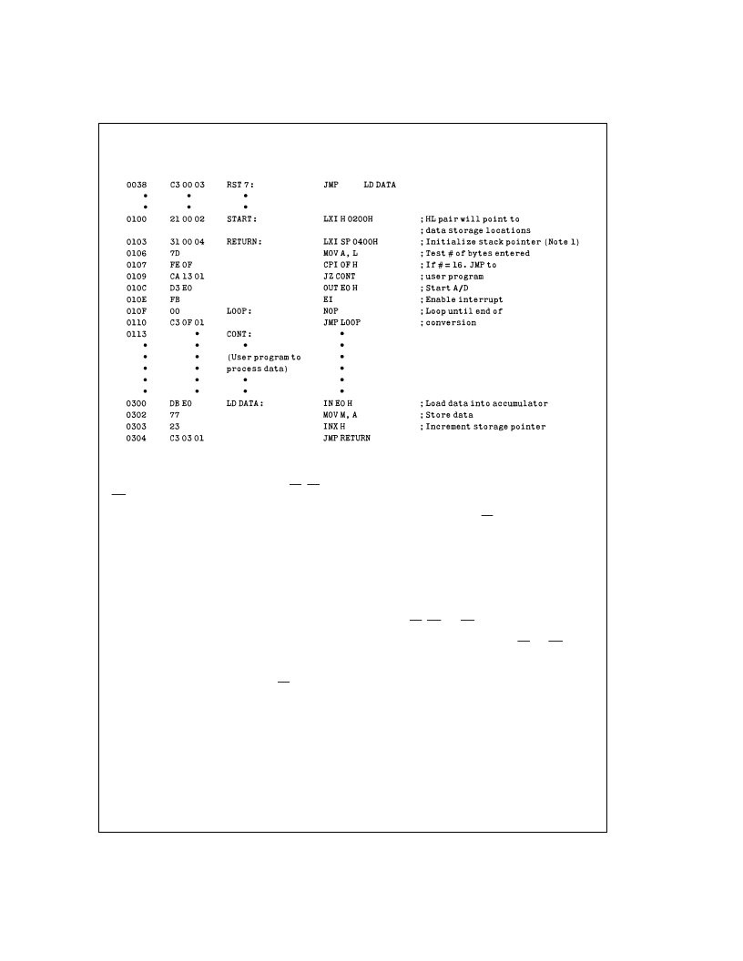
4.1.1 Sample 8080A CPU Interfacing Circuitry and
Program
The following sample program and associated hardware
shown in Figure 12 may be used to input data from the con-
verter to the INS8080A CPU chip set (comprised of the
INS8080A microprocessor, the INS8228 system controller
and the INS8224 clock generator). For simplicity, the A/D is
controlled as an I/O device, specifically an 8-bit bi-directional
port located at an arbitrarily chosen port address, E0. The
TRI-STATE output capability of the A/D eliminates the need
for a peripheral interface device, however address decoding
is still required to generate the appropriate CS for the con-
verter.
It is important to note that in systems where the A/D con-
verter is 1-of-8 or less I/O mapped devices, no address de-
coding circuitry is necessary. Each of the 8 address bits (A0
to A7) can be directly used as CS inputs— one for each I/O
device.
4.1.2 INS8048 Interface
The INS8048 interface technique with the ADC0801 series
(see Figure 13) is simpler than the 8080A CPU interface.
There are 24 I/O lines and three test input lines in the 8048.
With these extra I/O lines available, one of the I/O lines (bit
0 of port 1) is used as the chip select signal to the A/D, thus
eliminating the use of an external address decoder. Bus con-
trol signals RD, WR and INT of the 8048 are tied directly to
the A/D. The 16 converted data words are stored at on-chip
RAM locations from 20 to 2F (Hex). The RD and WR signals
are generated by reading from and writing into a dummy ad-
dress, respectively. A sample interface program is shown
below.
SAMPLE PROGRAM FOR
Figure 12
ADC0801–INS8080A CPU INTERFACE
DS005671-99
A
www.national.com
27
相关PDF资料 |
PDF描述 |
|---|---|
| ADC0802LD | 8-Bit, Microprocessor- Compatible, A/D Converters |
| ADC0804 | 8-Bit, Microprocessor-Compatible A/D Converters |
| ADC08060 | 8-Bit, 20 MSPS to 60 MSPS, 1.3 mW/MSPS A/D Converter |
| ADC08060CIMT | 8-Bit, 20 MSPS to 60 MSPS, 1.3 mW/MSPS A/D Converter |
| ADC0806 | 8-Bit, 20 MSPS to 60 MSPS, 1.3 mW/MSPS A/D Converter |
相关代理商/技术参数 |
参数描述 |
|---|---|
| ADC0802LCN/A+ | 制造商:未知厂家 制造商全称:未知厂家 功能描述:Analog-to-Digital Converter, 8-Bit |
| ADC0802LCN/NOPB | 功能描述:模数转换器 - ADC RoHS:否 制造商:Texas Instruments 通道数量:2 结构:Sigma-Delta 转换速率:125 SPs to 8 KSPs 分辨率:24 bit 输入类型:Differential 信噪比:107 dB 接口类型:SPI 工作电源电压:1.7 V to 3.6 V, 2.7 V to 5.25 V 最大工作温度:+ 85 C 安装风格:SMD/SMT 封装 / 箱体:VQFN-32 |
| ADC0802LCN-P | 功能描述:IC ADC 8BIT MPU COMPAT 20-DIP 制造商:texas instruments 系列:- 零件状态:最後搶購 位数:8 采样率(每秒):10k 输入数:1 输入类型:差分 数据接口:并联 配置:ADC 无线电 - S/H:ADC:- A/D 转换器数:1 架构:SAR 参考类型:外部,电源 电压 - 电源,模拟:4.5 V ~ 6.3 V 电压 - 电源,数字:4.5 V ~ 6.3 V 特性:- 工作温度:- 基本零件编号:ADC0802 标准包装:18 |
| ADC0802LCV | 制造商:未知厂家 制造商全称:未知厂家 功能描述:Analog-to-Digital Converter, 8-Bit |
| ADC0802LCWM | 制造商:Texas Instruments 功能描述: |
发布紧急采购,3分钟左右您将得到回复。