- 您现在的位置:买卖IC网 > PDF目录378277 > ADC0804 (National Semiconductor Corporation) 8-BitμP Compatible A/D Converters(8位μP 兼容A/D转换器) PDF资料下载
参数资料
| 型号: | ADC0804 |
| 厂商: | National Semiconductor Corporation |
| 元件分类: | 串行ADC |
| 英文描述: | 8-BitμP Compatible A/D Converters(8位μP 兼容A/D转换器) |
| 中文描述: | 8BitμP兼容的A / D转换器(8位微处理器兼容的A / D转换器) |
| 文件页数: | 19/41页 |
| 文件大小: | 1118K |
| 代理商: | ADC0804 |
第1页第2页第3页第4页第5页第6页第7页第8页第9页第10页第11页第12页第13页第14页第15页第16页第17页第18页当前第19页第20页第21页第22页第23页第24页第25页第26页第27页第28页第29页第30页第31页第32页第33页第34页第35页第36页第37页第38页第39页第40页第41页
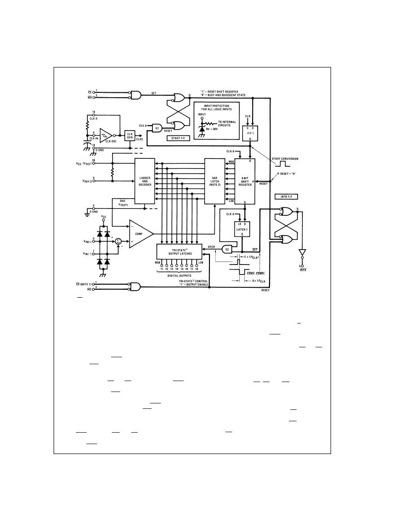
Functional Description
(Continued)
After the “1” is clocked through the 8-bit shift register (which
completes the SAR search) it appears as the input to the
D-type latch, LATCH 1. As soon as this “1” is output from the
shift register, the AND gate, G2, causes the new digital word
to transfer to the TRI-STATE output latches. When LATCH 1
is subsequently enabled, the Q output makes a high-to-low
transition which causes the INTR F/F to set. An inverting
buffer then supplies the INTR input signal.
Note that this SET control of the INTR F/F remains low for 8
of the external clock periods (as the internal clocks run at
1
8
of the frequency of the external clock). If the data output is
continuously enabled (CS and RD both held low), the INTR
output will still signal the end of conversion (by a high-to-low
transition), because the SET input can control the Q output
of the INTR F/F even though the RESET input is constantly
at a “1” level in this operating mode. This INTR output will
therefore stay low for the duration of the SET signal, which is
8 periods of the external clock frequency (assuming the A/D
is not started during this interval).
When operating in the free-running or continuous conversion
mode (INTR pin tied to WR and CS wired low— see also
section 2.8), the START F/F is SET by the high-to-low tran-
sition of the INTR signal. This resets the SHIFT REGISTER
which causes the input to the D-type latch, LATCH 1, to go
low.As the latch enable input is still present, the Q output will
go high, which then allows the INTR F/F to be RESET. This
reduces the width of the resulting INTR output pulse to only
a few propagation delays (approximately 300 ns).
When data is to be read, the combination of both CS and RD
being low will cause the INTR F/F to be reset and the
TRI-STATE output latches will be enabled to provide the 8-bit
digital outputs.
2.1 Digital Control Inputs
The digital control inputs (CS, RD, and WR) meet standard
T
2
L logic voltage levels. These signals have been renamed
when compared to the standardA/D Start and Output Enable
labels. In addition, these inputs are active low to allow an
easy interface to microprocessor control busses. For
non-microprocessor based applications, the CS input (pin 1)
can be grounded and the standard A/D Start function is ob-
tained by an active low pulse applied at the WR input (pin 3)
and the Output Enable function is caused by an active low
pulse at the RD input (pin 2).
DS005671-13
Note 13:
CS shown twice for clarity.
Note 14:
SAR = Successive Approximation Register.
FIGURE 4. Block Diagram
A
www.national.com
19
相关PDF资料 |
PDF描述 |
|---|---|
| ADC0805LCN | 8-Bit uP Compatible A/D Converters |
| ADC0801 | 8-Bit uP Compatible A/D Converters |
| ADC0802 | 8-Bit uP Compatible A/D Converters |
| ADC0802LCN | 8-Bit uP Compatible A/D Converters |
| ADC0805 | 8-Bit uP Compatible A/D Converters |
相关代理商/技术参数 |
参数描述 |
|---|---|
| ADC0804/D DIE | 制造商:Harris Corporation 功能描述: |
| ADC0804-1CD | 制造商:PHILIPS 制造商全称:NXP Semiconductors 功能描述:CMOS 8-bit A/D converters |
| ADC0804-1CN | 制造商:PHILIPS 制造商全称:NXP Semiconductors 功能描述:CMOS 8-bit A/D converters |
| ADC0804-1LCD | 制造商:PHILIPS 制造商全称:NXP Semiconductors 功能描述:CMOS 8-bit A/D converters |
| ADC0804-1LCN | 制造商:NXP Semiconductors 功能描述:Analog Digital Converter, Single, 8 Bit, 20 Pin, DIP |
发布紧急采购,3分钟左右您将得到回复。