- 您现在的位置:买卖IC网 > PDF目录378279 > ADC0833CCN (NATIONAL SEMICONDUCTOR CORP) 8-Bit Serial I/O A/D Converter with 4-Channel Multiplexer PDF资料下载
参数资料
| 型号: | ADC0833CCN |
| 厂商: | NATIONAL SEMICONDUCTOR CORP |
| 元件分类: | ADC |
| 英文描述: | 8-Bit Serial I/O A/D Converter with 4-Channel Multiplexer |
| 中文描述: | 4-CH 8-BIT SUCCESSIVE APPROXIMATION ADC, SERIAL ACCESS, PDIP14 |
| 封装: | 0.300 INCH, PLASTIC, DIP-14 |
| 文件页数: | 11/20页 |
| 文件大小: | 316K |
| 代理商: | ADC0833CCN |
Functional Description
(Continued)
4. When the start bit has been shifted into the start location
of the MUX register, the input channel has been assigned
and a conversion is about to begin. An interval of
(/2
clock
period (where nothing happens) is automatically inserted to
allow the selected MUX channel to settle. The SAR status
line goes high at this time to signal that a conversion is now
in progress and the DI line is disabled (it no longer accepts
data).
5. The data out (DO) line now comes out of TRI-STATE and
provides a leading zero for this one clock period of MUX
settling time.
6. When the conversion begins, the output of the SAR com-
parator, which indicates whether the analog input is greater
than (high) or less than (low) each successive voltage from
the internal resistor ladder, appears at the DO line on each
falling edge of the clock. This data is the result of the con-
version being shifted out (with the MSB coming first) and
can be read by the processor immediately.
7. After 8 clock periods the conversion is completed. The
SAR status line returns low to indicate this
(/2
clock cycle
later.
8. If the programmer prefers, the data can be read in an LSB
first format. All 8 bits of the result are stored in an output
shift register. The conversion result, LSB first, is automati-
cally shifted out the DO line, after the MSB first data stream.
The DO line then goes low and stays low until CS is re-
turned high.
9. All internal registers are cleared when the CS line is high.
If another conversion is desired, CS must make a high to
low transition followed by address information.
The DI and DO lines can be tied together and controlled
through a bidirectional processor I/O bit with one wire. This
is possible because the DI input is only ‘‘looked-at’’ during
the MUX addressing interval while the DO line is still in a
high impedance state.
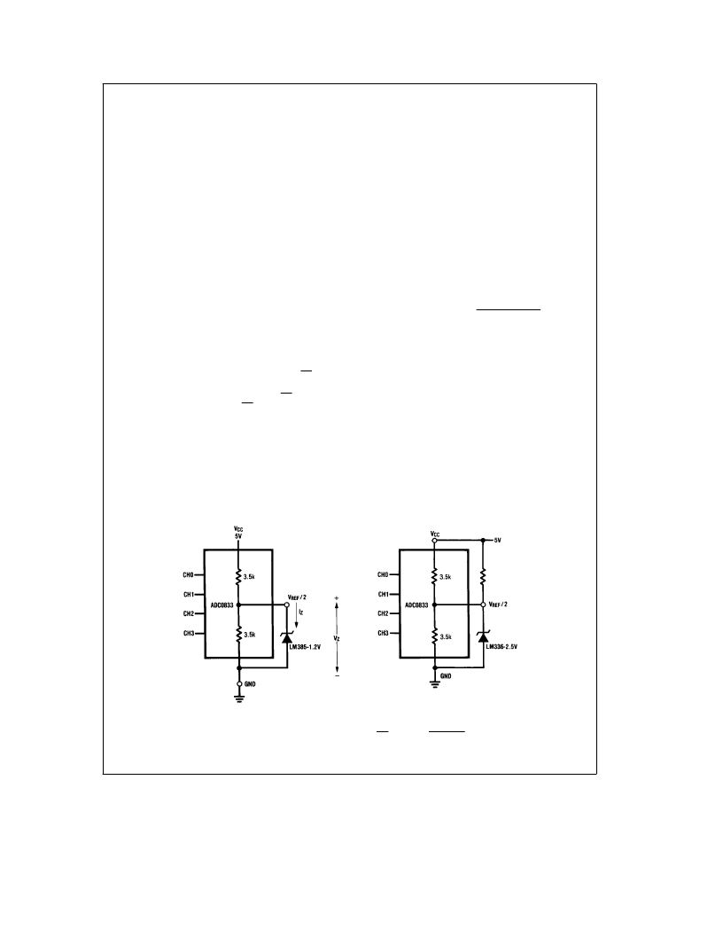
3.0 REFERENCE CONSIDERATIONS
The ADC0833 is intended primarily for use in circuits requir-
ing absolute accuracy. In this type of system, the analog
inputs vary between very specific voltage limits and the ref-
erence voltage for the A/D converter must remain stable
with time and temperature. For ratiometric applications, an
ADC0834 is a pin-for-pin compatible alternative since it has
a V
REF
input (note the ADC0834 needs one less bit of mux
addressing information).
The voltage applied to the V
REF
/2 pin defines the voltage
span of the analog input
[
the difference between V
IN
(
a
)
and V
IN
(
b
)
]
over which the 256 possible output codes ap-
ply. A full-scale conversion (an all 1s output code) will result
when the voltage difference between a selected ‘‘
a
’’ input
and ‘‘
b
’’ input is approximately twice the voltage at the
V
REF
/2 pin. This internal gain of 2 from the applied refer-
ence to the full-scale input voltage allows biasing a low volt-
age reference diode from the 5V
DC
converter supply. To
accommodate a 5V input span, only a 2.5V reference is
required. The LM385 and LM336 reference diodes are good
low current devices to use with these converters. The out-
put code changes in accordance with the following equa-
tion:
Output Code
e
256
V
IN
(
a
)
b
V
IN
(
b
)
2(V
REF
/2)
where the output code is the decimal equivalent of the 8-bit
binary output (ranging from 0 to 255) and the term V
REF
/2 is
the voltage from pin 9 to ground.
The V
REF
/2 pin is the center point of a two resistor divider
(each resistor is 3.5 k
X
) connected from V
CC
to ground.
Total ladder input resistance is the sum of these two equal
resistors. As shown in Figure 2, a reference diode with a
voltage less than V
CC
/2 can be connected without requiring
an external biasing resistor if its current requirements meet
the indicated level.
The minimum value of V
REF
/2 can be quite small (see Typi-
cal Performance Characteristics) to allow direct conversions
of transducer outputs providing less than a 5V output span.
Particular care must be taken with regard to noise pickup,
circuit layout and system error voltage sources when oper-
ating with a reduced span due to the increased sensitivity of
the converter (1 LSB equals V
REF
/256).
TL/H/5607–7
V
FULL-SCALE
j
2.4V
Note:
No external biasing resistor needed if V
Z
k
V
CC
V
FULL-SCALE
j
5.0V
and I
Z
min
k
V
CC
/2
b
V
Z
2
1.75 k
X
FIGURE 2. Reference Biasing Examples
11
相关PDF资料 |
PDF描述 |
|---|---|
| ADC08351 | 8-Bit, 42 MSPS, 40 mW A/D Converter |
| ADC08351CIMTC | 8-Bit, 42 MSPS, 40 mW A/D Converter |
| ADC08351CIMTCX | 8-Bit, 42 MSPS, 40 mW A/D Converter |
| ADC0841 | 8-Bit P Compatible A/D Converter |
| ADC0841BCN | 8-Bit P Compatible A/D Converter |
相关代理商/技术参数 |
参数描述 |
|---|---|
| ADC0833CCN/A+ | 制造商:未知厂家 制造商全称:未知厂家 功能描述:Analog-to-Digital Converter, 8-Bit |
| ADC0833CCN/B+ | 制造商:未知厂家 制造商全称:未知厂家 功能描述:Analog-to-Digital Converter, 8-Bit |
| ADC0833CJ | 制造商:未知厂家 制造商全称:未知厂家 功能描述:Analog-to-Digital Converter, 8-Bit |
| ADC0834 | 制造商:NSC 制造商全称:National Semiconductor 功能描述:8-Bit Serial I/O A/D Converters with Multiplexer Options |
| ADC0834A | 制造商:TI 制造商全称:Texas Instruments 功能描述:A/D PERIPHERALS WITH SERIAL CONTROL |
发布紧急采购,3分钟左右您将得到回复。