- 您现在的位置:买卖IC网 > PDF目录378279 > ADC08351CIMTCX (NATIONAL SEMICONDUCTOR CORP) 8-Bit, 42 MSPS, 40 mW A/D Converter PDF资料下载
参数资料
| 型号: | ADC08351CIMTCX |
| 厂商: | NATIONAL SEMICONDUCTOR CORP |
| 元件分类: | ADC |
| 英文描述: | 8-Bit, 42 MSPS, 40 mW A/D Converter |
| 中文描述: | 1-CH 8-BIT RESISTANCE LADDER ADC, PARALLEL ACCESS, PDSO20 |
| 封装: | TSSOP-20 |
| 文件页数: | 10/15页 |
| 文件大小: | 492K |
| 代理商: | ADC08351CIMTCX |
Applications Information
(Continued)
the analog supply pin should be minimized, keeping it below
200 mV
at 100 kHz. Of course, higher frequency noise on
the power supply should be even more severely limited.
No pin should ever have a voltage on it that is in excess of
the supply voltages. This can be a problem upon application
of power to a circuit. Be sure that the supplies to circuits driv-
ing the CLK, OE, analog input and reference pins do not
come up any faster than does the voltage at the ADC08351
power pins.
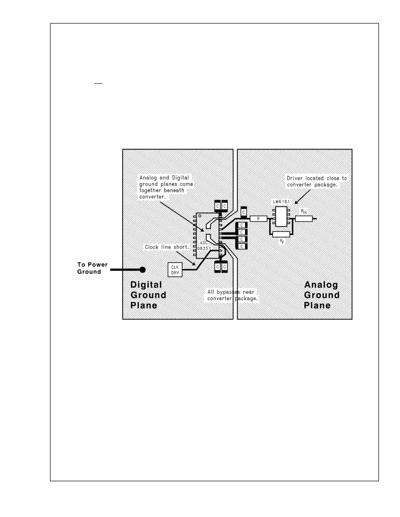
3.0 LAYOUT AND GROUNDING
Proper grounding and proper routing of all signals is essen-
tial to ensure accurate conversion. Separate analog and
digital ground planes that are connected beneath the
ADC08351 are required to meet data sheet limits. The ana-
log and digital grounds may be in the same layer, but should
be separated from each other and should
never
overlap
each other.
Capacitive coupling between the typically noisy digital
ground plane and the sensitive analog circuitry can lead to
poor performance that may seem impossible to isolate and
remedy. The solution is to keep the analog circuitry well
separated from the digital circuitry and from the digital
ground plane.
Generally, analog and digital lines should cross each other at
90 degrees to avoid getting digital noise into the analog path.
To maximize accuracy in video (high frequency) systems,
however, avoid crossing analog and digital lines altogether.
Furthermore, it is important to keep any clock lines isolated
from ALL other lines, including other digital lines. Even the
generally accepted 90 degree crossing should be avoided as
even a little coupling can cause problems at high frequen-
cies.
Best performance at high frequencies and at high resolution
is obtained with a straight signal path. That is, the signal path
through all components should form a straight line wherever
possible.
Be especially careful with the layout of inductors. Mutual in-
ductance can change the characteristics of the circuit in
which they are used. Inductors should not be placed side by
side, even with just a small part of their bodies beside each
other.
The analog input should be isolated from noisy signal traces
to avoid coupling of spurious signals into the input. Any ex-
ternal component (e.g., a filter capacitor) connected be-
tween the converter’s input and ground should be connected
to a very clean point in the analog ground plane.
Figure 3gives an example of a suitable layout.All analog cir-
cuitry (input amplifiers, filters, reference components, etc.)
should be placed on or over the analog ground plane. All
digital circuitry and I/O lines should be placed over the digital
ground plane.
All ground connections should have a low inductance path to
ground.
4.0 DYNAMIC PERFORMANCE
The ADC08351 is ac tested and its dynamic performance is
guaranteed. To meet the published specifications, the clock
source driving the CLK input must be free of jitter. For best
DS100895-25
FIGURE 3. Layout example showing separate analog and digital ground planes connected below the ADC08351.
A
www.national.com
10
相关PDF资料 |
PDF描述 |
|---|---|
| ADC0841 | 8-Bit P Compatible A/D Converter |
| ADC0841BCN | 8-Bit P Compatible A/D Converter |
| ADC0841BCV | 8-Bit P Compatible A/D Converter |
| ADC0841CCN | 8-Bit P Compatible A/D Converter |
| ADC0841CCV | 8-Bit P Compatible A/D Converter |
相关代理商/技术参数 |
参数描述 |
|---|---|
| ADC08351CIMTCX/NOPB | 功能描述:模数转换器 - ADC RoHS:否 制造商:Texas Instruments 通道数量:2 结构:Sigma-Delta 转换速率:125 SPs to 8 KSPs 分辨率:24 bit 输入类型:Differential 信噪比:107 dB 接口类型:SPI 工作电源电压:1.7 V to 3.6 V, 2.7 V to 5.25 V 最大工作温度:+ 85 C 安装风格:SMD/SMT 封装 / 箱体:VQFN-32 |
| ADC08351EVAL | 功能描述:EVALUATION BOARD FOR ADC08351 RoHS:是 类别:编程器,开发系统 >> 过时/停产零件编号 系列:- 标准包装:1 系列:- 传感器类型:CMOS 成像,彩色(RGB) 传感范围:WVGA 接口:I²C 灵敏度:60 fps 电源电压:5.7 V ~ 6.3 V 嵌入式:否 已供物品:成像器板 已用 IC / 零件:KAC-00401 相关产品:4H2099-ND - SENSOR IMAGE WVGA COLOR 48-PQFP4H2094-ND - SENSOR IMAGE WVGA MONO 48-PQFP |
| ADC08351EVM | 功能描述:ADC08351EVM 制造商:texas instruments 系列:* 零件状态:在售 标准包装:1 |
| ADC0838 | 制造商:MICRO-LINEAR 制造商全称:MICRO-LINEAR 功能描述:Serial I/O 8-Bit A/D Converters with Multiplexer Options |
| ADC0838A | 制造商:TI 制造商全称:Texas Instruments 功能描述:A/D PERIPHERALS WITH SERIAL CONTROL |
发布紧急采购,3分钟左右您将得到回复。