- 您现在的位置:买卖IC网 > PDF目录378279 > ADC08351CIMTCX (NATIONAL SEMICONDUCTOR CORP) 8-Bit, 42 MSPS, 40 mW A/D Converter PDF资料下载
参数资料
| 型号: | ADC08351CIMTCX |
| 厂商: | NATIONAL SEMICONDUCTOR CORP |
| 元件分类: | ADC |
| 英文描述: | 8-Bit, 42 MSPS, 40 mW A/D Converter |
| 中文描述: | 1-CH 8-BIT RESISTANCE LADDER ADC, PARALLEL ACCESS, PDSO20 |
| 封装: | TSSOP-20 |
| 文件页数: | 5/15页 |
| 文件大小: | 492K |
| 代理商: | ADC08351CIMTCX |
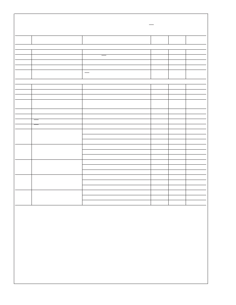
Converter Electrical Characteristics
(Continued)
The following specifications apply for V
= V
= +3.0 V
, V
REF
= 2.4V, V
IN
= 1.63 V
P-P
, OE = 0V, C
L
= 20 pF,
f
= 42 MHz, 50% duty cycle, unless otherwise specified.
Boldface limits apply for T
A
= T
MIN
to T
MAX
:
all other limits T
A
= 25C (Notes 7, 8)
Symbol
Parameter
Conditions
Typical
(Note 9)
Limits
(Note 9)
Units
(Limits)
Digital Output Characteristics
I
OH
High Level Output Current
I
OL
Low Level Output Current
V
OH
High Level Output Voltage
V
OL
Low Level Output Voltage
I
OZH
,
I
OZL
AC Electrical Characteristics
f
C1
Maximum Conversion Rate
f
C2
Minimum Conversion Rate
t
OD
Output Delay
V
D
= 2.7V, V
OH
= V
D
0.5V
V
D
= 2.7V, OE = DGND, V
OL
= 0.4V
V
D
= 2.7V, I
OH
= 360 μA
V
D
= 2.7V, I
OL
= 1.6 mA
1.1
1.8
mA (min)
mA (min)
V
V
2.65
0.2
TRI-STATE Output Current
OE = V
D
= 3.3V, V
OH
= 3.3V or V
OL
= 0V
±
10
μA
42
MHz (min)
MHz
ns (max)
Clock
Cycles
ns
ns
ns
ns
Bits
Bits
Bits (min)
dB
dB
dB (min)
dB
dB
dB (min)
dB
dB
dB (min)
dB
dB
dB (min)
2
14
CLK High to Data Valid
19
Pipline Delay (Latency)
2.5
t
DS
t
OH
t
EN
t
DIS
Sampling (Aperture) Delay
Output Hold Time
OE Low to Data Valid
OE High to High Z State
CLK Low to Acquisition of Data
CLK High to Data Invalid
Loaded as in Figure 2
Loaded as in Figure 2
f
CLK
= 30 MHz, f
IN
= 1 MHz
f
CLK
= 42 MHz, f
IN
= 4.4 MHz
f
CLK
= 42 MHz, f
IN
= 21 MHz
f
CLK
= 30 MHz, f
IN
= 1 MHz
f
CLK
= 42 MHz, f
IN
= 4.4 MHz
f
CLK
= 42 MHz, f
IN
= 21 MHz
f
CLK
= 30 MHz, f
IN
= 1 MHz
f
CLK
= 42 MHz, f
IN
= 4.4 MHz
f
CLK
= 42 MHz, f
IN
= 21 MHz
f
CLK
= 30 MHz, f
IN
= 1 MHz
f
CLK
= 42 MHz, f
IN
= 4.4 MHz
f
CLK
= 42 MHz, f
IN
= 21 MHz
f
CLK
= 30 MHz, f
IN
= 1 MHz
f
CLK
= 42 MHz, f
IN
= 4.4 MHz
f
CLK
= 42 MHz, f
IN
= 21 MHz
2
9
14
10
7.2
7.2
6.8
45
45
43
44
45
44
57
51
46
57
54
49
ENOB
Effective Number of Bits
6.1
SINAD
Signal-to-Noise & Distortion
38.5
SNR
Signal-to-Noise Ratio
41
THD
Total Harmonic Distortion
41
SFDR
Spurious Free Dynamic Range
41
Note 1:
Absolute Maximum Ratings indicate limits beyond which damage to the device may occur. Operating Ratings indicate conditions for which the device is func-
tional, but do not guarantee specific performance limits. For guaranteed specifications and test conditions, see the Electrical Characteristics. The guaranteed speci-
fications apply only for the test conditions listed. Some performance characteristics may degrade when the device is not operated under the listed test conditions.
Note 2:
All voltages are measured with respect to GND = AGND = DGND = 0V, unless otherwise specified.
Note 3:
When the input voltage at any pin exceeds the power supplies (that is, less than AGND or DGND, or greater than V
A
or V
D
), the current at that pin should
be limited to 25 mA. The 50 mA maximum package input current rating limits the number of pins that can safely exceed the power supplies with an input current of
25 mA to two.
Note 4:
The absolute maximum junction temperature (T
max) for this device is 150C. The maximum allowable power dissipation is dictated by T
max, the
junction-to-ambient thermal resistance (
θ
), and the ambient temperature (T
), and can be calculated using the formula P
MAX = (T
max - T
)/
θ
. For the 20-pin
TSSOP,
θ
is 135C/W, so P
MAX = 926 mW at 25C and 481 mW at the maximum operating ambient temperature of 85C. Note that the power dissipation of this
device under normal operation will typically be about 68 mW (40 mW quiescent power + 23 mW reference ladder power + 5 mW due to 1 TTL loan on each digital
output). The values for maximum power dissipation listed above will be reached only when the ADC08351 is operated in a severe fault condition (e.g., when input
or output pins are driven beyond the power supply voltages, or the power supply polarity is reversed). Obviously, such conditions should always be avoided.
Note 5:
Human body model is 100 pF capacitor discharged through a 1.5 k
resistor. Machine model is 220 pF discharged through ZERO Ohms.
Note 6:
See AN-450, “Surface Mounting Methods and Their Effect on Product Reliability”, or the section entitled “Surface Mount” found in any post 1986 National
Semiconductor Linear Data Book, for other methods of soldering surface mount devices.
Note 7:
All inputs are protected as shown below. Input voltage magnitudes up to 500 mV above the supply voltage or 500 mV below GND will not damage this device.
However, errors in the A/D conversion can occur if the input goes above V
A
or below AGND by more than 300 mV. As an example, if V
A
is 3.0 V
DC
, the full-scale
input voltage must be
≤
3.3 V
DC
to ensure accurate conversions.
A
www.national.com
5
相关PDF资料 |
PDF描述 |
|---|---|
| ADC0841 | 8-Bit P Compatible A/D Converter |
| ADC0841BCN | 8-Bit P Compatible A/D Converter |
| ADC0841BCV | 8-Bit P Compatible A/D Converter |
| ADC0841CCN | 8-Bit P Compatible A/D Converter |
| ADC0841CCV | 8-Bit P Compatible A/D Converter |
相关代理商/技术参数 |
参数描述 |
|---|---|
| ADC08351CIMTCX/NOPB | 功能描述:模数转换器 - ADC RoHS:否 制造商:Texas Instruments 通道数量:2 结构:Sigma-Delta 转换速率:125 SPs to 8 KSPs 分辨率:24 bit 输入类型:Differential 信噪比:107 dB 接口类型:SPI 工作电源电压:1.7 V to 3.6 V, 2.7 V to 5.25 V 最大工作温度:+ 85 C 安装风格:SMD/SMT 封装 / 箱体:VQFN-32 |
| ADC08351EVAL | 功能描述:EVALUATION BOARD FOR ADC08351 RoHS:是 类别:编程器,开发系统 >> 过时/停产零件编号 系列:- 标准包装:1 系列:- 传感器类型:CMOS 成像,彩色(RGB) 传感范围:WVGA 接口:I²C 灵敏度:60 fps 电源电压:5.7 V ~ 6.3 V 嵌入式:否 已供物品:成像器板 已用 IC / 零件:KAC-00401 相关产品:4H2099-ND - SENSOR IMAGE WVGA COLOR 48-PQFP4H2094-ND - SENSOR IMAGE WVGA MONO 48-PQFP |
| ADC08351EVM | 功能描述:ADC08351EVM 制造商:texas instruments 系列:* 零件状态:在售 标准包装:1 |
| ADC0838 | 制造商:MICRO-LINEAR 制造商全称:MICRO-LINEAR 功能描述:Serial I/O 8-Bit A/D Converters with Multiplexer Options |
| ADC0838A | 制造商:TI 制造商全称:Texas Instruments 功能描述:A/D PERIPHERALS WITH SERIAL CONTROL |
发布紧急采购,3分钟左右您将得到回复。