- 您现在的位置:买卖IC网 > PDF目录10737 > ADCMP605BCPZ-WP (Analog Devices Inc)IC COMP TTL/CMOS 1CHAN 12LFCSP PDF资料下载
参数资料
| 型号: | ADCMP605BCPZ-WP |
| 厂商: | Analog Devices Inc |
| 文件页数: | 14/16页 |
| 文件大小: | 0K |
| 描述: | IC COMP TTL/CMOS 1CHAN 12LFCSP |
| 标准包装: | 50 |
| 类型: | 带锁销 |
| 元件数: | 1 |
| 输出类型: | 补充型,LVDS,满摆幅 |
| 电压 - 电源,单路/双路(±): | 2.5 V ~ 5.5 V |
| 电压 - 输入偏移(最小值): | 5mV @ 3V |
| 电流 - 输入偏压(最小值): | 5µA @ 3V |
| 电流 - 输出(标准): | 50mA |
| 电流 - 静态(最大值): | 3mA |
| CMRR, PSRR(标准): | 50dB CMRR,50dB PSRR |
| 传输延迟(最大): | 3ns |
| 磁滞: | 100µV |
| 工作温度: | -40°C ~ 125°C |
| 封装/外壳: | 12-VFQFN 裸露焊盘,CSP |
| 安装类型: | 表面贴装 |
| 包装: | 托盘 - 晶粒 |
ADCMP604/ADCMP605
Rev. A | Page 7 of 16
PIN CONFIGURATION AND FUNCTION DESCRIPTIONS
ADCMP604
TOP VIEW
(Not to Scale)
Q 1
Q
6
VEE 2
VCCI/VCCO
5
VP 3
VN
4
05
916
-00
2
Figure 3. ADCMP604 Pin Configuration
Table 5. ADCMP604 Pin Function Descriptions (6-Lead SC70)
Pin No.
Mnemonic
Description
1
Q
Noninverting Output. Q is at logic high if the analog voltage at the noninverting input, VP, is greater than the
analog voltage at the inverting input, VN.
2
VEE
Negative Supply Voltage.
3
VP
Noninverting Analog Input.
4
VN
Inverting Analog Input.
5
VCCI/VCCO
Input Section Supply/Output Section Supply. VCCI and VCCO are shared pin.
6
Q
Inverting Output. Q is at logic low if the analog voltage at the noninverting input, VP, is greater than the analog
voltage at the inverting input, VN.
PIN 1
INDICATOR
TOP VIEW
(Not to Scale)
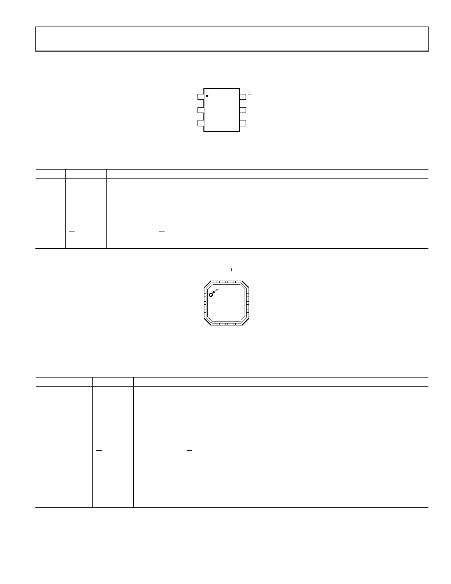
ADCMP605
VCCO 1
VCCI 2
VEE 3
V
P
4
V
EE
5
V
N
6
9 VEE
8 LE/HYS
7 SDN
12
Q
11
V
EE
10
Q
05
91
6-
00
3
Figure 4. ADCMP605 Pin Configuration
Table 6. ADCMP605 Pin Function Descriptions (12-Lead LFCSP_VQ)
Pin No.
Mnemonic
Description
1
VCCO
Output Section Supply.
2
VCCI
Input Section Supply.
3, 5, 9, 11
VEE
Negative Supply Voltages.
4
VP
Noninverting Analog Input.
6
VN
Inverting Analog Input.
7
SDN
Shutdown. Drive this pin low to shut down the device.
8
LE/HYS
Latch/Hysteresis Control. Bias with resistor or current for hysteresis; drive low to latch.
10
Q
Inverting Output. Q is at Logic low if the analog voltage at the noninverting input, VP, is greater than
the analog voltage at the inverting input, VN, if the comparator is in compare mode.
12
Q
Noninverting Output. Q is at Logic high if the analog voltage at the noninverting input, VP, is greater
than the analog voltage at the inverting input, VN, if the comparator is in compare mode.
Heat Sink Paddle
VEE
The metallic back surface of the package is electrically connected to VEE. It can be left floating
because Pin 3, Pin 5, Pin 9, and Pin 11 provide adequate electrical connection. It can also be
soldered to the application board if improved thermal and/or mechanical stability is desired.
相关PDF资料 |
PDF描述 |
|---|---|
| ADCMP563BRQZ | IC COMPARATOR ECL DUAL 16QSOP |
| VI-JNP-MY-F3 | CONVERTER MOD DC/DC 13.8V 50W |
| VI-BW0-MY-B1 | CONVERTER MOD DC/DC 5V 50W |
| VI-JNP-MY-F2 | CONVERTER MOD DC/DC 13.8V 50W |
| VI-B1H-MY-B1 | CONVERTER MOD DC/DC 52V 50W |
相关代理商/技术参数 |
参数描述 |
|---|---|
| ADCMP605BCPZ-WP1 | 制造商:AD 制造商全称:Analog Devices 功能描述:Rail-to-Rail, Very Fast, 2.5 V to 5.5 V, Single-Supply LVDS Comparators |
| ADCMP606 | 制造商:AD 制造商全称:Analog Devices 功能描述:Rail-to-Rail, Very Fast, 2.5 V to 5.5 V, Single-Supply CML Comparators |
| ADCMP606_0610 | 制造商:AD 制造商全称:Analog Devices 功能描述:Rail-to-Rail, Very Fast, 2.5 V to 5.5 V, Single-Supply CML Comparators |
| ADCMP606_07 | 制造商:AD 制造商全称:Analog Devices 功能描述:Rail-to-Rail, Very Fast, 2.5 V to 5.5 V, Single-Supply CML Comparators |
| ADCMP606BKSZ-R2 | 功能描述:IC COMP TTL/CMOS 1CHAN SC70-6 RoHS:是 类别:集成电路 (IC) >> 线性 - 比较器 系列:- 产品培训模块:Lead (SnPb) Finish for COTS Obsolescence Mitigation Program 标准包装:50 系列:- 类型:带电压基准 元件数:4 输出类型:开路漏极 电压 - 电源,单路/双路(±):2.5 V ~ 11 V,±1.25 V ~ 5.5 V 电压 - 输入偏移(最小值):10mV @ 5V 电流 - 输入偏压(最小值):- 电流 - 输出(标准):0.015mA @ 5V 电流 - 静态(最大值):8.5µA CMRR, PSRR(标准):80dB CMRR,80dB PSRR 传输延迟(最大):- 磁滞:- 工作温度:0°C ~ 70°C 封装/外壳:16-SOIC(0.154",3.90mm 宽) 安装类型:表面贴装 包装:管件 产品目录页面:1386 (CN2011-ZH PDF) |
发布紧急采购,3分钟左右您将得到回复。