- 您现在的位置:买卖IC网 > PDF目录10737 > ADCMP607BCPZ-WP (Analog Devices Inc)IC COMP TTL/CMOS 1CHAN 12-LFCSP PDF资料下载
参数资料
| 型号: | ADCMP607BCPZ-WP |
| 厂商: | Analog Devices Inc |
| 文件页数: | 2/16页 |
| 文件大小: | 0K |
| 描述: | IC COMP TTL/CMOS 1CHAN 12-LFCSP |
| 标准包装: | 50 |
| 类型: | 带锁销 |
| 元件数: | 1 |
| 输出类型: | CML,补充型,满摆幅 |
| 电压 - 电源,单路/双路(±): | 2.5 V ~ 5.5 V |
| 电压 - 输入偏移(最小值): | 5mV @ 2.5V |
| 电流 - 输入偏压(最小值): | 5µA @ 2.5V |
| 电流 - 输出(标准): | 50mA |
| 电流 - 静态(最大值): | 1.5mA |
| CMRR, PSRR(标准): | 50dB CMRR,50dB PSRR |
| 传输延迟(最大): | 2.1ns |
| 磁滞: | 100µV |
| 工作温度: | -40°C ~ 125°C |
| 封装/外壳: | 12-VFQFN 裸露焊盘,CSP |
| 安装类型: | 表面贴装 |
| 包装: | 托盘 - 晶粒 |
ADCMP606/ADCMP607
Rev. A | Page 10 of 16
APPLICATION INFORMATION
POWER/GROUND LAYOUT AND BYPASSING
The ADCMP606/ADCMP607 comparators are very high speed
devices. Despite the low noise output stage, it is essential to use
proper high speed design techniques to achieve the specified
performance. Because comparators are uncompensated amplifiers,
feedback in any phase relationship is likely to cause oscillations
or undesired hysteresis. Of critical importance is the use of low
impedance supply planes, particularly the output supply plane
(VCCO) and the ground plane (GND). Individual supply planes
are recommended as part of a multilayer board. Providing the
lowest inductance return path for switching currents ensures
the best possible performance in the target application.
It is also important to adequately bypass the input and output
supplies. Multiple high quality 0.01 μF bypass capacitors should
be placed as close as possible to each of the VCCI and VCCO supply
pins and should be connected to the GND plane with redundant
vias. At least one of these should be placed to provide a physically
short return path for output currents flowing back from ground
to the VCCI and VCCO pins. High frequency bypass capacitors
should be carefully selected for minimum inductance and ESR.
Parasitic layout inductance should also be strictly controlled to
maximize the effectiveness of the bypass at high frequencies.
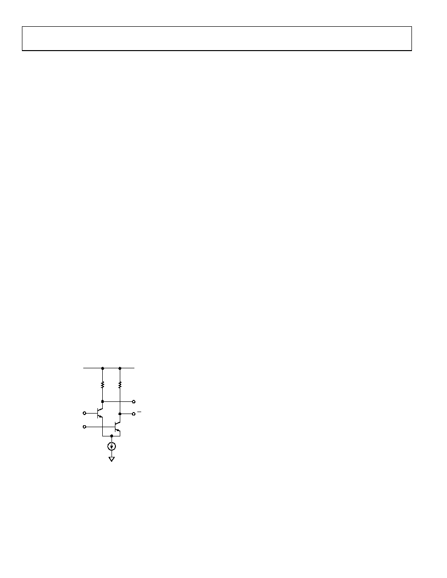
CML-COMPATIBLE OUTPUT STAGE
Specified propagation delay dispersion performance can be
achieved by using proper transmission line terminations. The
outputs of the ADCMP606 and ADCMP607 are designed to drive
400 mV directly into a 50 Ω cable or into transmission lines
terminated using either microstrip or strip line techniques with
50 Ω referenced to VCCO. The CML output stage is shown in the
simplified schematic diagram in Figure 14. Each output is back-
terminated with 50 Ω for best transmission line matching.
Q
16mA
50
Q
VCCO
GND
05
917
-01
3
Figure 14. Simplified Schematic Diagram of
CML-Compatible Output Stage
If these high speed signals must be routed more than a centimeter,
then either microstrip or strip line techniques are required to
ensure proper transition times and to prevent excessive output
ringing and pulse width dependent propagation delay
dispersion.
It is also possible to operate the outputs with the internal
termination only if greater output swing is desired. This can be
especially useful for driving inputs on CMOS devices intended
for full swing ECL and PECL, or for generating pseudo PECL
levels. To avoid deep saturation of the outputs and resulting
pulse dispersion, VCCO must be kept above the specified
minimum output low level (see the Electrical Characteristics
section). The line length driven should be kept as short as
possible.
USING/DISABLING THE LATCH FEATURE
The latch input is designed for maximum versatility. It can
safely be left floating or it can be driven low by any standard
TTL/CMOS device as a high speed latch.
In addition, the pin can be operated as a hysteresis control pin
with a bias voltage of 1.25 V nominal and an input resistance of
approximately 70 kΩ. This allows the comparator hysteresis to
be easily controlled by either a resistor or an inexpensive CMOS
DAC. Driving this pin high or floating the pin removes all
hysteresis.
Hysteresis control and latch mode can be used together if an
open-drain, an open-collector, or a three-state driver is con-
nected parallel to the hysteresis control resistor or current source.
Due to the programmable hysteresis feature, the logic threshold
of the latch pin is approximately 1.1 V regardless of VCCO.
OPTIMIZING PERFORMANCE
As with any high speed comparator, proper design and layout
techniques are essential for obtaining the specified performance.
Stray capacitance, inductance, inductive power and ground
impedances, or other layout issues can severely limit performance
and often cause oscillation. Large discontinuities along input
and output transmission lines can also limit the specified pulse
width dispersion performance. The source impedance should
be minimized as much as is practicable. High source impedance,
in combination with the parasitic input capacitance of the
comparator, causes an undesirable degradation in bandwidth at
the input, thus degrading the overall response. Thermal noise
from large resistances can easily cause extra jitter with slowly
slewing input signals; higher impedances encourage undesired
coupling.
相关PDF资料 |
PDF描述 |
|---|---|
| VI-JNR-MY-F4 | CONVERTER MOD DC/DC 7.5V 50W |
| VI-BWY-MW-B1 | CONVERTER MOD DC/DC 3.3V 66W |
| VI-JNR-MY-F2 | CONVERTER MOD DC/DC 7.5V 50W |
| VI-BWW-MY-B1 | CONVERTER MOD DC/DC 5.5V 50W |
| VI-JNR-MY-F1 | CONVERTER MOD DC/DC 7.5V 50W |
相关代理商/技术参数 |
参数描述 |
|---|---|
| ADCMP608 | 制造商:AD 制造商全称:Analog Devices 功能描述:Rail-to-Rail, Fast, Low Power 2.5 V to 5.5 V, Single-Supply TTL/CMOS Comparator |
| ADCMP608_07 | 制造商:AD 制造商全称:Analog Devices 功能描述:Rail-to-Rail, Fast, Low Power 2.5 V to 5.5 V, Single-Supply TTL/CMOS Comparator |
| ADCMP608BKSZ-R2 | 功能描述:IC COMP TTL/CMOS R-R SGL SC70-6 RoHS:是 类别:集成电路 (IC) >> 线性 - 比较器 系列:- 标准包装:25 系列:- 类型:带电压基准 元件数:4 输出类型:CMOS,开路漏极,TTL 电压 - 电源,单路/双路(±):2 V ~ 11 V,±1 V ~ 5.5 V 电压 - 输入偏移(最小值):10mV @ 5V 电流 - 输入偏压(最小值):- 电流 - 输出(标准):0.015mA @ 5V 电流 - 静态(最大值):8.5µA CMRR, PSRR(标准):80dB CMRR,80dB PSRR 传输延迟(最大):12µs 磁滞:50mV 工作温度:0°C ~ 70°C 封装/外壳:16-DIP(0.300",7.62mm) 安装类型:通孔 包装:管件 |
| ADCMP608BKSZ-REEL | 制造商:AD 制造商全称:Analog Devices 功能描述:Rail-to-Rail, Fast, Low Power 2.5 V to 5.5 V, Single-Supply TTL/CMOS Comparator |
| ADCMP608BKSZ-REEL7 | 功能描述:IC COMPARATOR TTL/CMOS SC70-6 RoHS:是 类别:集成电路 (IC) >> 线性 - 比较器 系列:- 标准包装:1 系列:- 类型:通用 元件数:1 输出类型:CMOS,开路集电极,TTL 电压 - 电源,单路/双路(±):2.7 V ~ 5.5 V 电压 - 输入偏移(最小值):7mV @ 5V 电流 - 输入偏压(最小值):0.25µA @ 5V 电流 - 输出(标准):84mA @ 5V 电流 - 静态(最大值):120µA CMRR, PSRR(标准):- 传输延迟(最大):600ns 磁滞:- 工作温度:-40°C ~ 85°C 封装/外壳:SC-74A,SOT-753 安装类型:表面贴装 包装:剪切带 (CT) 产品目录页面:1268 (CN2011-ZH PDF) 其它名称:*LMV331M5*LMV331M5/NOPBLMV331M5CT |
发布紧急采购,3分钟左右您将得到回复。