- 您现在的位置:买卖IC网 > PDF目录9103 > ADF4154BRU-REEL7 (Analog Devices Inc)IC FRACTION-N FREQ SYNTH 16TSSOP PDF资料下载
参数资料
| 型号: | ADF4154BRU-REEL7 |
| 厂商: | Analog Devices Inc |
| 文件页数: | 13/24页 |
| 文件大小: | 0K |
| 描述: | IC FRACTION-N FREQ SYNTH 16TSSOP |
| 标准包装: | 1,000 |
| 类型: | 分数 N 合成器(RF) |
| PLL: | 是 |
| 输入: | CMOS,TTL |
| 输出: | 时钟 |
| 电路数: | 1 |
| 比率 - 输入:输出: | 2:1 |
| 差分 - 输入:输出: | 是/无 |
| 频率 - 最大: | 4GHz |
| 除法器/乘法器: | 无/是 |
| 电源电压: | 2.7 V ~ 3.3 V |
| 工作温度: | -40°C ~ 85°C |
| 安装类型: | 表面贴装 |
| 封装/外壳: | 16-TSSOP(0.173",4.40mm 宽) |
| 供应商设备封装: | 16-TSSOP |
| 包装: | 带卷 (TR) |
| 配用: | EVAL-ADF4154EBZ1-ND - BOARD EVALUATION FOR ADF4154EB1 |
ADF4154
Data Sheet
Rev. C | Page 20 of 24
In low spur mode (dither enabled), the repeat length is
extended to 221 cycles, regardless of the value of MOD, which
makes the quantization error spectrum appear as broadband
noise. This can degrade the in-band phase noise at the PLL
output by as much as 10 dB. Therefore, for lowest noise, dither
off is a better choice, particularly when the final loop BW is low
enough to attenuate even the lowest frequency fractional spur.
Integer Boundary Spurs
Another mechanism for fractional spur creation are interactions
between the RF VCO frequency and the reference frequency.
When these frequencies are not integer related (as is the case
with fractional-N synthesizers), spur sidebands appear on the
VCO output spectrum at an offset frequency that corresponds
to the beat note or the difference in frequency between an
integer multiple of the reference and the VCO frequency.
These spurs are attenuated by the loop filter and are more
noticeable on channels close to integer multiples of the
reference, where the difference frequency can be inside the loop
bandwidth, thus the name integer boundary spurs.
Reference Spurs
Reference spurs are generally not a problem in fractional-N
synthesizers because the reference offset is far outside the loop
bandwidth. However, any reference feedthrough mechanism
that bypasses the loop can cause a problem. One such
mechanism is feedthrough of low levels of on-chip reference
switching noise through the RFIN pin back to the VCO, resulting
in reference spur levels as high as –90 dBc. Care should be
taken in the PCB layout to ensure that the VCO is well
separated from the input reference to avoid a possible feed-
through path on the board.
SPUR CONSISTENCY
When jumping from Frequency A to Frequency B and then
back again using fractional-N synthesizers, the spur levels often
differ each time Frequency A is programmed. However, in the
ADF4154, the spur levels on any particular channel are always
consistent.
FILTER DESIGN—ADIsimPLL
A filter design and analysis program is available to help the user
implement the PLL design. Visit www.analog.com/pll for a free
download of the ADIsimPLL software. The software designs,
simulates, and analyzes the entire PLL frequency and time
domain response. Various passive and active filter architectures
are allowed.
INTERFACING
The ADF4154 has a simple, SPI-compatible serial interface for
writing to the device. SCLK, SDATA, and LE control the data
transfer. When LE (latch enable) is high, the 22 bits that have
been clocked into the input register on each rising edge of
SCLK are transferred to the appropriate latch. See Figure 2 for
the timing diagram and Table 5 for the latch truth table.
The maximum allowable serial clock rate is 20 MHz. This
means that the maximum update rate possible for the device is
909 kHz or one update every 1.1 s.
ADuC812 Interface
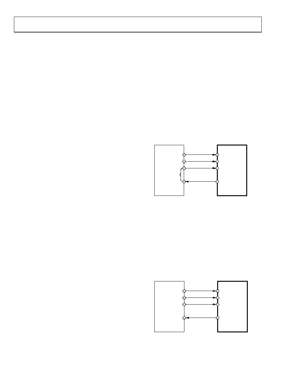
Figure 21 shows the interface between the ADF4154 and the
ADuC812 MicroConverter. Because the ADuC812 is based on
an 8051 core, this interface can be used with any 8051-based
microcontroller. The MicroConverter is set up for SPI master
mode with CPHA set to 0. To initiate the operation, bring the
I/O port driving LE low. Each latch of the ADF4154 requires a
24-bit word, which is accomplished by writing three 8-bit bytes
from the MicroConverter to the device. After the third byte is
written, the LE input should be brought high to complete the
transfer.
When operating in the mode described, the maximum
SCLOCK rate of the ADuC812 is 4 MHz. This means that the
maximum rate at which the output frequency can be changed is
180 kHz.
ADuC812
ADF4154
SCLOCK
SCLK
SDATA
LE
MUXOUT
(LOCK DETECT)
MOSI
I/O PORTS
04833-
024
Figure 21. ADuC812-to-ADF4154 Interface
ADSP-21xx Interface
Figure 22 shows the interface between the ADF4154 and the
ADSP-21xx digital signal processor. As discussed previously, the
ADF4154 requires a 24-bit serial word for each latch write. The
easiest way to accomplish this using a device in the ADSP-21xx
family is to use the autobuffered transmit mode of operation
with alternate framing. This provides a means for transmitting
an entire block of serial data before an interrupt is generated.
Set up the word length for eight bits and use three memory
locations for each 24-bit word. To program each 24-bit latch,
store each of the three 8-bit bytes, enable the autobuffered
mode, and write to the transmit register of the DSP. This last
operation initiates the autobuffered transfer.
ADSP-21xx
ADF4154
SCLOCK
SCLK
SDATA
LE
MUXOUT
(LOCK DETECT)
DT
TFS
I/O FLAGS
04833-
025
Figure 22. ADSP-21xx-to-ADF4154 Interface
相关PDF资料 |
PDF描述 |
|---|---|
| MS3450L28-11PW | CONN RCPT 22POS WALL MNT W/PINS |
| X9317UP-2.7 | IC XDCP 100TAP 50K 3-WIRE 8-DIP |
| X9317TV8T1 | IC XDCP 100TAP 100K 3WIRE 8TSSOP |
| X9317TV8IT2 | IC XDCP 100TAP 100K 3WIRE 8TSSOP |
| MS3450L28-11P | CONN RCPT 22POS WALL MNT W/PINS |
相关代理商/技术参数 |
参数描述 |
|---|---|
| ADF4154BRUZ | 功能描述:IC FRAC-N FREQ SYNTH 16-TSSOP RoHS:是 类别:集成电路 (IC) >> 时钟/计时 - 时钟发生器,PLL,频率合成器 系列:- 标准包装:2,000 系列:- 类型:PLL 频率合成器 PLL:是 输入:晶体 输出:时钟 电路数:1 比率 - 输入:输出:1:1 差分 - 输入:输出:无/无 频率 - 最大:1GHz 除法器/乘法器:是/无 电源电压:4.5 V ~ 5.5 V 工作温度:-20°C ~ 85°C 安装类型:表面贴装 封装/外壳:16-LSSOP(0.175",4.40mm 宽) 供应商设备封装:16-SSOP 包装:带卷 (TR) 其它名称:NJW1504V-TE1-NDNJW1504V-TE1TR |
| ADF4154BRUZ-RL | 功能描述:IC FRACTION-N FREQ SYNTH 16TSSOP RoHS:是 类别:集成电路 (IC) >> 时钟/计时 - 时钟发生器,PLL,频率合成器 系列:- 标准包装:1,000 系列:Precision Edge® 类型:时钟/频率合成器 PLL:无 输入:CML,PECL 输出:CML 电路数:1 比率 - 输入:输出:2:1 差分 - 输入:输出:是/是 频率 - 最大:10.7GHz 除法器/乘法器:无/无 电源电压:2.375 V ~ 3.6 V 工作温度:-40°C ~ 85°C 安装类型:表面贴装 封装/外壳:16-VFQFN 裸露焊盘,16-MLF? 供应商设备封装:16-MLF?(3x3) 包装:带卷 (TR) 其它名称:SY58052UMGTRSY58052UMGTR-ND |
| ADF4154BRUZ-RL7 | 功能描述:IC FRACTION-N FREQ SYNTH 16TSSOP RoHS:是 类别:集成电路 (IC) >> 时钟/计时 - 时钟发生器,PLL,频率合成器 系列:- 标准包装:2,000 系列:- 类型:PLL 频率合成器 PLL:是 输入:晶体 输出:时钟 电路数:1 比率 - 输入:输出:1:1 差分 - 输入:输出:无/无 频率 - 最大:1GHz 除法器/乘法器:是/无 电源电压:4.5 V ~ 5.5 V 工作温度:-20°C ~ 85°C 安装类型:表面贴装 封装/外壳:16-LSSOP(0.175",4.40mm 宽) 供应商设备封装:16-SSOP 包装:带卷 (TR) 其它名称:NJW1504V-TE1-NDNJW1504V-TE1TR |
| ADF4155BCPZ | 功能描述:IC PLL FRAC-N FREQ SYNTH 20LFCSP 制造商:analog devices inc. 系列:- 包装:托盘 零件状态:有效 类型:* PLL:是 输入:LVDS,LVPECL 输出:时钟 电路数:1 比率 - 输入:输出:2:1 差分 - 输入:输出:是/无 频率 - 最大值:4GHz 分频器/倍频器:是/无 电压 - 电源:3.135 V ~ 3.465 V 工作温度:-40°C ~ 85°C 安装类型:表面贴装 封装/外壳:24-WFQFN 裸露焊盘,CSP 供应商器件封装:24-LFCSP-WQ(4x4) 标准包装:1 |
| ADF4155BCPZ-RL7 | 功能描述:IC PLL FRAC-N FREQ SYNTH 20LFCSP 制造商:analog devices inc. 系列:- 包装:带卷(TR) 零件状态:有效 类型:* PLL:是 输入:LVDS,LVPECL 输出:时钟 电路数:1 比率 - 输入:输出:2:1 差分 - 输入:输出:是/无 频率 - 最大值:4GHz 分频器/倍频器:是/是 电压 - 电源:3.135 V ~ 3.465 V 工作温度:-40°C ~ 85°C 安装类型:表面贴装 封装/外壳:24-WFQFN 裸露焊盘,CSP 供应商器件封装:24-LFCSP-WQ(4x4) 标准包装:1,500 |
发布紧急采购,3分钟左右您将得到回复。