- 您现在的位置:买卖IC网 > PDF目录1989 > ADF4193BCPZ-RL7 (Analog Devices Inc)IC PLL FREQ SYNTHESIZER 32LFCSP PDF资料下载
参数资料
| 型号: | ADF4193BCPZ-RL7 |
| 厂商: | Analog Devices Inc |
| 文件页数: | 20/32页 |
| 文件大小: | 0K |
| 描述: | IC PLL FREQ SYNTHESIZER 32LFCSP |
| 标准包装: | 1,500 |
| 类型: | 时钟/频率合成器,RF |
| PLL: | 是 |
| 输入: | CMOS,TTL |
| 输出: | 时钟 |
| 电路数: | 1 |
| 比率 - 输入:输出: | 2:1 |
| 差分 - 输入:输出: | 是/无 |
| 频率 - 最大: | 3.5GHz |
| 除法器/乘法器: | 是/是 |
| 电源电压: | 2.7 V ~ 3.3 V |
| 工作温度: | -40°C ~ 85°C |
| 安装类型: | 表面贴装 |
| 封装/外壳: | 32-VFQFN 裸露焊盘,CSP |
| 供应商设备封装: | 32-LFCSP-VQ(5x5) |
| 包装: | 带卷 (TR) |
| 配用: | EVAL-ADF4193EBZ2-ND - BOARD EVALUATION EB2 FOR ADF4193 EVAL-ADF4193EBZ1-ND - BOARD EVALUATION EB1 FOR ADF4193 |
第1页第2页第3页第4页第5页第6页第7页第8页第9页第10页第11页第12页第13页第14页第15页第16页第17页第18页第19页当前第20页第21页第22页第23页第24页第25页第26页第27页第28页第29页第30页第31页第32页
Data Sheet
ADF4193
Rev. F | Page 27 of 32
INTERFACING
The ADF4193 has a simple SPI-compatible serial interface for
writing to the device. CLK, DATA, and LE control the data
transfer. When LE goes high, the 24 bits that have been clocked
into the input register on each rising edge of CLK are latched
into the appropriate register. See Figure 2 for the timing
diagram and Table 5 for the register address table.
The maximum allowable serial clock rate is 33 MHz.
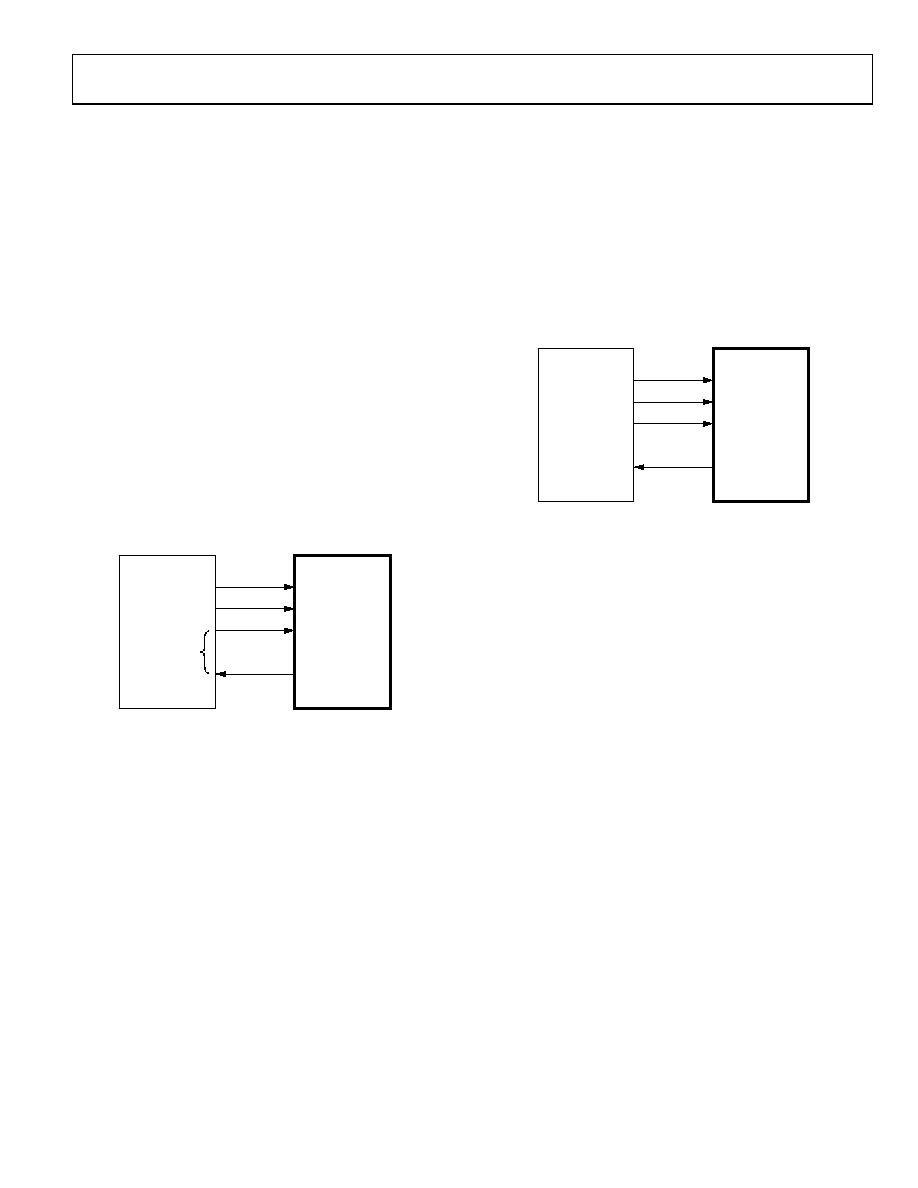
ADuC812 Interface
Figure 37 shows the interface between the ADF4193 and the
an 8051 core, this interface can be used with any 8051-based
microcontroller. The MicroConverter is set up for SPI master
mode with CPHA = 0. To initiate the operation, the I/O port
driving LE is brought low. Some registers of the ADF4193
require a 24-bit programming word. This is accomplished by
writing three 8-bit bytes from the MicroConverter to the device.
When the third byte is written, the LE input should be brought
high to complete the transfer.
An I/O port line on the ADuC812 can also be used to detect
lock (MUXOUT configured as lock detect and polled by the
port input).
ADuC812
ADF4193
SCLOCK
CLK
DATA
LE
MUXOUT
(LOCK DETECT)
MOSI
I/O PORTS
05328-
033
Figure 37. ADuC812 to ADF4193 Interface
ADSP-21xx Interface
Figure 38 shows the interface between the ADF4193 and the
ADSP-21xx digital signal processor. The ADF4193 needs a
24-bit serial word for some writes. The easiest way to accom-
plish this using the ADSP-21xx family is to use the autobuffered
transmit mode of operation with alternate framing. This
provides a means for transmitting an entire block of serial data
before an interrupt is generated. Set up the word length for
eight bits and use three memory locations for each 24-bit word.
To program each 24-bit word, store the three 8-bit bytes, enable
the autobuffered mode, and then write to the transmit register
of the DSP. This last operation initiates the autobuffer transfer.
ADSP-21xx
ADF4193
SCLK
CLK
DATA
LE
MUXOUT
(LOCK DETECT)
DT
TFS
I/O FLAGS
05328-
034
Figure 38. ADSP-21xx to ADF4193 Interface
PCB DESIGN GUIDELINES FOR CHIP SCALE
PACKAGE
The lands on the chip scale package (CP-32-3) are rectangular.
The printed circuit board (PCB) pad for these should be 0.1 mm
longer than the package land length and 0.05 mm wider than
the package land width. The land should be centered on the
pad. This ensures that the solder joint size is maximized. The
bottom of the chip scale package has a central thermal pad.
The thermal pad on the PCB should be at least as large as the
exposed pad. On the PCB, there should be a clearance of at least
0.25 mm between the thermal pad and the inner edges of the
pad pattern. This ensures that shorting is avoided.
Thermal vias can be used on the PCB thermal pad to improve
the thermal performance of the package. If vias are used, they
should be incorporated in the thermal pad at 1.2 mm pitch grid.
The via diameter should be between 0.3 mm and 0.33 mm, and
the via barrel should be plated with one ounce copper to plug
the via.
The user should connect the PCB thermal pad to AGND.
相关PDF资料 |
PDF描述 |
|---|---|
| ADF4206BRUZ-RL | IC PLL FREQ SYNTHESIZER 16TSSOP |
| ADF4212LBRUZ | IC PLL FREQ SYNTHESIZER 20TSSOP |
| ADF4213BCPZ-RL | IC PLL FREQ SYNTHESIZER 20LFCSP |
| ADF4216BRUZ-RL | IC PLL FREQ SYNTHESIZER 20TSSOP |
| ADF4218LBRUZ | IC PLL FREQ SYNTHESIZER 20TSSOP |
相关代理商/技术参数 |
参数描述 |
|---|---|
| ADF4193SP1BCPZ | 制造商:Analog Devices 功能描述: |
| ADF4193SP1BCPZ-RL7 | 制造商:Analog Devices 功能描述: |
| ADF4193SP2BCPZ-RL7 | 制造商:Analog Devices 功能描述: |
| ADF4193WCCPZ-RL7 | 功能描述:IC PLL FREQ SYNTHESIZER 32LFCSP RoHS:是 类别:集成电路 (IC) >> 时钟/计时 - 时钟发生器,PLL,频率合成器 系列:- 标准包装:2,000 系列:- 类型:PLL 时钟发生器 PLL:带旁路 输入:LVCMOS,LVPECL 输出:LVCMOS 电路数:1 比率 - 输入:输出:2:11 差分 - 输入:输出:是/无 频率 - 最大:240MHz 除法器/乘法器:是/无 电源电压:3.135 V ~ 3.465 V 工作温度:0°C ~ 70°C 安装类型:表面贴装 封装/外壳:32-LQFP 供应商设备封装:32-TQFP(7x7) 包装:带卷 (TR) |
| ADF4196 | 制造商:AD 制造商全称:Analog Devices 功能描述:Low Phase Noise, Fast Settling, 6 GHz |
发布紧急采购,3分钟左右您将得到回复。