- 您现在的位置:买卖IC网 > PDF目录9108 > ADF4212BRUZ-RL7 (Analog Devices Inc)IC PLL FREQ SYNTHESIZER 20-TSSOP PDF资料下载
参数资料
| 型号: | ADF4212BRUZ-RL7 |
| 厂商: | Analog Devices Inc |
| 文件页数: | 10/20页 |
| 文件大小: | 0K |
| 描述: | IC PLL FREQ SYNTHESIZER 20-TSSOP |
| 标准包装: | 1,000 |
| 类型: | 时钟/频率合成器(RF/IF) |
| PLL: | 是 |
| 输入: | CMOS,TTL |
| 输出: | 时钟 |
| 电路数: | 1 |
| 比率 - 输入:输出: | 3:1 |
| 差分 - 输入:输出: | 是/无 |
| 频率 - 最大: | 2.7GHz |
| 除法器/乘法器: | 无/无 |
| 电源电压: | 2.7 V ~ 5.5 V |
| 工作温度: | -40°C ~ 85°C |
| 安装类型: | 表面贴装 |
| 封装/外壳: | 20-TSSOP(0.173",4.40mm 宽) |
| 供应商设备封装: | 20-TSSOP |
| 包装: | 带卷 (TR) |
REV. A
ADF4210/ADF4211/ADF4212/ADF4213
–18–
VP
VDD2
ADF4213
VP2
3.9nF
470
130pF
20k
27nF
M3500-1324
VCC
18
100pF
18
RFOUT
1000pF 1000pF
51
REFIN
MUXOUT
LOCK
DETECT
51
100pF
AGND
IF
DGND
IF
RFIN
CE
CLK
DATA
LE
SPI-COMPATIBLE
SERIAL
BUS
DECOUPLING CAPACITORS ON VDD, VP OF THE ADF4213,
ON VCC OF THE AD820 AND ON THE VCC OF THE M3500-1324
HAVE BEEN OMITTED FROM THE DIAGRAM TO AID CLARITY.
THE IF SECTION OF THE CIRCUIT HAS ALSO BEEN OMITTED TO
SIMPLIFY THE SCHEMATIC.
RSET
CPRF
2.7k
12V
V_TUNE
GND
20V
1k
AD820
3k
OUT
FREFIN
VDD
VP1
VDD1
DGND
RF
AGND
RF
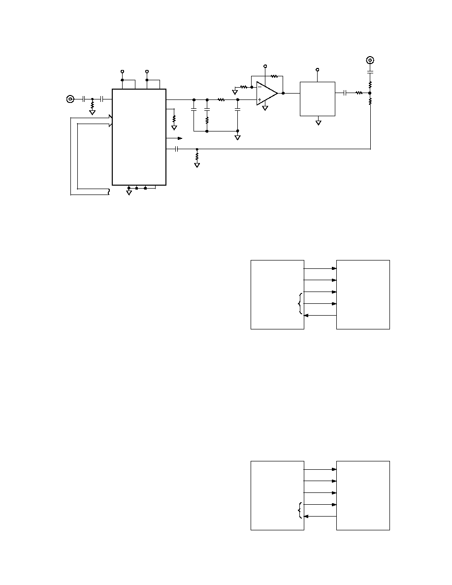
Figure 8. Wideband PLL Circuit
in wide-band applications both of these parameters have a much
greater variation. In Figure 8, for example, we have –25% and
+30% variation in the RF output from the nominal 1.8 GHz.
The sensitivity of the VCO can vary from 130 MHz/V at
1900 MHz to 30 MHz/V at 2400 MHz. Variations in these
parameters will change the loop bandwidth. This in turn can
affect stability and lock time. By changing the programmable
ICP, it is possible to obtain compensation for these varying
loop conditions and ensure that the loop is always operating
close to optimal conditions.
INTERFACING
The ADF4210/ADF4211/ADF4212/ADF4213 family has a
simple SPI-compatible serial interface for writing to the device.
SCLK, SDATA, and LE control the data transfer. When LE
(Latch Enable) goes high, the 22 bits that have been clocked
into the input register on each rising edge of SCLK will be
transferred to the appropriate latch. See Figure 1 for the Timing
Diagram and Table I for the Latch Truth Table.
The maximum allowable serial clock rate is 20 MHz. This
means that the maximum update rate possible for the device is
909 kHz, or one update every 1.1 ms. This is certainly more
than adequate for systems that will have typical lock times in
hundreds of microseconds.
ADuC812 to ADF421x Family Interface
Figure 9 shows the interface between the ADF421x family and
the ADuC812 microconverter. Since the ADuC812 is based on
an 8051 core, this interface can be used with any 8051-based
microcontroller. The microconverter is set up for SPI Master
Mode with CPHA = 0. To initiate the operation, the I/O port
driving LE is brought low. Each latch of the ADF421x family
needs a 24-bit word. This is accomplished by writing three 8-bit
bytes from the microconverter to the device. When the third
byte has been written, the LE input should be brought high to
complete the transfer.
On rst applying power to the ADF421x family, it needs four
writes (one each to the R counter latch and the AB counter latch
for both RF1 and RF2 sides) for the output to become active.
When operating in the mode described, the maximum SCLOCK
rate of the ADuC812 is 4 MHz. This means that the maximum
rate at which the output frequency can be changed will be about
180 kHz.
SCLOCK
MOSI
I/O PORTS
ADuC812
SCLK
SDATA
LE
CE
MUXOUT
(LOCK DETECT)
ADF4210/
ADF4211/
ADF4212/
ADF4213
Figure 9. ADuC812 to ADF421x Family Interface
ADSP-21xx to ADF421x Family Interface
Figure 10 shows the interface between the ADF421x family and
the ADSP-21xx Digital Signal Processor. As previously discussed,
the ADF421x family needs a 24-bit serial word for each latch
write. The easiest way to accomplish this, using the ADSP-21xx
family, is to use the Autobuffered Transmit Mode of operation
with Alternate Framing. This provides a means for transmitting
an entire block of serial data before an interrupt is generated.
Set up the word length for eight bits and use three memory
locations for each 24-bit word. To program each 24-bit latch,
store the three 8-bit bytes, enable the Autobuffered mode, and
write to the transmit register of the DSP. This last operation
initiates the autobuffer transfer.
SCLK
DT
I/O FLAGS
ADSP-21xx
SCLK
SDATA
LE
CE
MUXOUT
(LOCK DETECT)
ADF4210/
ADF4211/
ADF4212/
ADF4213
TFS
Figure 10. ADSP-21xx to ADF421x Family Interface
相关PDF资料 |
PDF描述 |
|---|---|
| ADF4212LBCPZ-RL7 | IC PLL FREQ SYNTHESIZER 20LFCSP |
| ADF4212LBRUZ-RL7 | IC PLL FREQ SYNTHESIZER 20TSSOP |
| ADF4106BRU-REEL | IC PLL FREQ SYNTHESIZER 16-TSSOP |
| ADF4212LBCPZ-RL | IC PLL FREQ SYNTHESIZER 20LFCSP |
| ADF4212BRUZ-RL | IC PLL FREQ SYNTHESIZER 20-TSSOP |
相关代理商/技术参数 |
参数描述 |
|---|---|
| ADF4212L | 制造商:AD 制造商全称:Analog Devices 功能描述:Dual Low Power PLL Frequency Synthesizer |
| ADF4212LBCP | 制造商:AD 制造商全称:Analog Devices 功能描述:Dual Low Power PLL Frequency Synthesizer |
| ADF4212LBCPZ | 功能描述:IC PLL FREQ SYNTHESIZER 20LFCSP RoHS:是 类别:集成电路 (IC) >> 时钟/计时 - 时钟发生器,PLL,频率合成器 系列:- 标准包装:1,000 系列:Precision Edge® 类型:时钟/频率合成器 PLL:无 输入:CML,PECL 输出:CML 电路数:1 比率 - 输入:输出:2:1 差分 - 输入:输出:是/是 频率 - 最大:10.7GHz 除法器/乘法器:无/无 电源电压:2.375 V ~ 3.6 V 工作温度:-40°C ~ 85°C 安装类型:表面贴装 封装/外壳:16-VFQFN 裸露焊盘,16-MLF? 供应商设备封装:16-MLF?(3x3) 包装:带卷 (TR) 其它名称:SY58052UMGTRSY58052UMGTR-ND |
| ADF4212LBCPZ-RL | 功能描述:IC PLL FREQ SYNTHESIZER 20LFCSP RoHS:是 类别:集成电路 (IC) >> 时钟/计时 - 时钟发生器,PLL,频率合成器 系列:- 标准包装:1,000 系列:Precision Edge® 类型:时钟/频率合成器 PLL:无 输入:CML,PECL 输出:CML 电路数:1 比率 - 输入:输出:2:1 差分 - 输入:输出:是/是 频率 - 最大:10.7GHz 除法器/乘法器:无/无 电源电压:2.375 V ~ 3.6 V 工作温度:-40°C ~ 85°C 安装类型:表面贴装 封装/外壳:16-VFQFN 裸露焊盘,16-MLF? 供应商设备封装:16-MLF?(3x3) 包装:带卷 (TR) 其它名称:SY58052UMGTRSY58052UMGTR-ND |
| ADF4212LBCPZ-RL7 | 功能描述:IC PLL FREQ SYNTHESIZER 20LFCSP RoHS:是 类别:集成电路 (IC) >> 时钟/计时 - 时钟发生器,PLL,频率合成器 系列:- 标准包装:1,000 系列:Precision Edge® 类型:时钟/频率合成器 PLL:无 输入:CML,PECL 输出:CML 电路数:1 比率 - 输入:输出:2:1 差分 - 输入:输出:是/是 频率 - 最大:10.7GHz 除法器/乘法器:无/无 电源电压:2.375 V ~ 3.6 V 工作温度:-40°C ~ 85°C 安装类型:表面贴装 封装/外壳:16-VFQFN 裸露焊盘,16-MLF? 供应商设备封装:16-MLF?(3x3) 包装:带卷 (TR) 其它名称:SY58052UMGTRSY58052UMGTR-ND |
发布紧急采购,3分钟左右您将得到回复。