参数资料
| 型号: | ADF4360-1BCPZ |
| 厂商: | Analog Devices Inc |
| 文件页数: | 3/24页 |
| 文件大小: | 0K |
| 描述: | IC SYNTHESIZER VCO 24-LFCSP |
| 标准包装: | 1 |
| 类型: | 扇出配送,整数-N,合成器(RF) |
| PLL: | 是 |
| 输入: | CMOS,TTL |
| 输出: | 时钟 |
| 电路数: | 1 |
| 比率 - 输入:输出: | 1:2 |
| 差分 - 输入:输出: | 无/无 |
| 频率 - 最大: | 2.45GHz |
| 除法器/乘法器: | 是/无 |
| 电源电压: | 3 V ~ 3.6 V |
| 工作温度: | -40°C ~ 85°C |
| 安装类型: | 表面贴装 |
| 封装/外壳: | 24-VFQFN 裸露焊盘,CSP |
| 供应商设备封装: | 24-LFCSP-VQ(4x4) |
| 包装: | 托盘 |
| 产品目录页面: | 551 (CN2011-ZH PDF) |
| 配用: | EVAL-ADF4360-1EBZ1-ND - BOARD EVALUATION FOR ADF4360-1 |
Data Sheet
ADF4360-1
Rev. C | Page 11 of 24
After band select, normal PLL action resumes. The nominal value
of KV is 57 MHz/V or 28 MHZ/V if divide-by-2 operation has been
selected (by programming DIV2 [DB22], high in the N counter
latch). The ADF4360 family contains linearization circuitry to min-
imize any variation of the product of ICP and KV.
The operating current in the VCO core is programmable in four
steps: 5 mA, 10 mA, 15 mA, and 20 mA. This is controlled by
Bits PC1 and PC2 in the control latch.
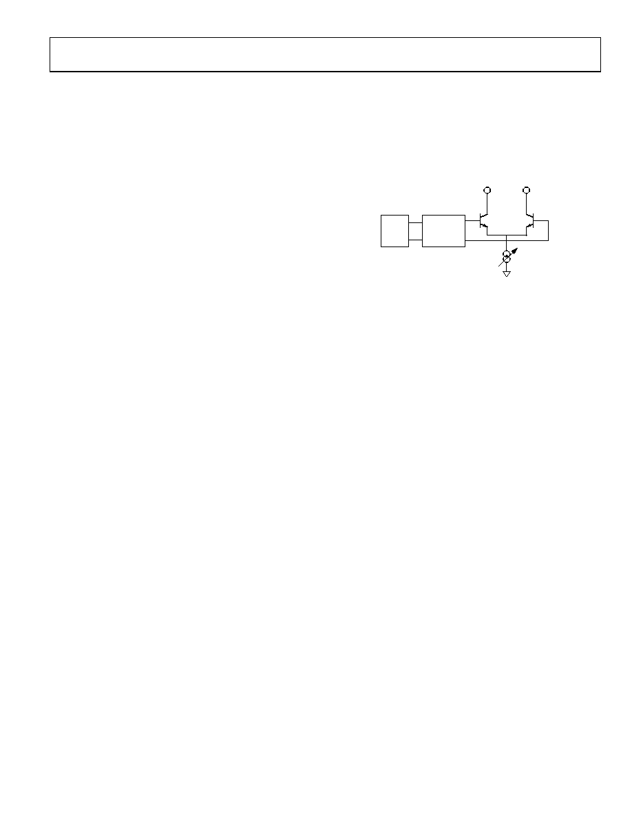
OUTPUT STAGE
The RFOUTA and RFOUTB pins of the ADF4360 family are con-
nected to the collectors of an NPN differential pair driven by
buffered outputs of the VCO, as shown in Figure 15. To allow
the user to optimize the power dissipation versus the output
power requirements, the tail current of the differential pair is
programmable via Bits PL1 and PL2 in the control latch. Four
current levels may be set: 3.5 mA, 5 mA, 7.5 mA, and 11 mA.
These levels give output power levels of 13 dBm, 10.5 dBm,
8 dBm, and 6 dBm, respectively, using a 50 resistor to VDD
and ac coupling into a 50 load. Alternatively, both outputs
can be combined in a 1 + 1:1 transformer or a 180° microstrip
coupler (see the Output Matching section).
If the outputs are used individually, the optimum output stage
consists of a shunt inductor to VDD.
Another feature of the ADF4360 family is that the supply current
to the RF output stage is shut down until the part achieves lock as
measured by the digital lock detect circuitry. This is enabled by the
mute-till-lock detect (MTLD) bit in the control latch.
VCO
RFOUTA
RFOUTB
BUFFER/
DIVIDE BY 2
04414-015
Figure 15. Output Stage ADF4360-1
相关PDF资料 |
PDF描述 |
|---|---|
| VE-24B-MX-B1 | CONVERTER MOD DC/DC 95V 75W |
| VE-J1Z-MZ-S | CONVERTER MOD DC/DC 2V 10W |
| VE-243-MX-B1 | CONVERTER MOD DC/DC 24V 75W |
| X9317WV8Z-2.7 | IC XDCP SGL 100TAP 10K 8-TSSOP |
| VE-J1Y-MZ-S | CONVERTER MOD DC/DC 3.3V 16.5W |
相关代理商/技术参数 |
参数描述 |
|---|---|
| ADF4360-1BCPZ | 制造商:Analog Devices 功能描述:INTEGRATED SYNTHESIZER |
| ADF4360-1BCPZ | 制造商:Analog Devices 功能描述:IC FREQ SYNTHESIZER 2450MHZ 24-LFCSP |
| ADF4360-1BCPZRL | 功能描述:IC SYNTHESIZER VCO 24LFCSP RoHS:是 类别:集成电路 (IC) >> 时钟/计时 - 时钟发生器,PLL,频率合成器 系列:- 标准包装:1,000 系列:Precision Edge® 类型:时钟/频率合成器 PLL:无 输入:CML,PECL 输出:CML 电路数:1 比率 - 输入:输出:2:1 差分 - 输入:输出:是/是 频率 - 最大:10.7GHz 除法器/乘法器:无/无 电源电压:2.375 V ~ 3.6 V 工作温度:-40°C ~ 85°C 安装类型:表面贴装 封装/外壳:16-VFQFN 裸露焊盘,16-MLF? 供应商设备封装:16-MLF?(3x3) 包装:带卷 (TR) 其它名称:SY58052UMGTRSY58052UMGTR-ND |
| ADF4360-1BCPZRL7 | 功能描述:IC SYNTHESIZER VCO 24LFCSP RoHS:是 类别:集成电路 (IC) >> 时钟/计时 - 时钟发生器,PLL,频率合成器 系列:- 标准包装:1,000 系列:Precision Edge® 类型:时钟/频率合成器 PLL:无 输入:CML,PECL 输出:CML 电路数:1 比率 - 输入:输出:2:1 差分 - 输入:输出:是/是 频率 - 最大:10.7GHz 除法器/乘法器:无/无 电源电压:2.375 V ~ 3.6 V 工作温度:-40°C ~ 85°C 安装类型:表面贴装 封装/外壳:16-VFQFN 裸露焊盘,16-MLF? 供应商设备封装:16-MLF?(3x3) 包装:带卷 (TR) 其它名称:SY58052UMGTRSY58052UMGTR-ND |
| ADF4360-1SP1BCPZ | 制造商:Analog Devices 功能描述: |
发布紧急采购,3分钟左右您将得到回复。