- 您现在的位置:买卖IC网 > PDF目录17099 > ADM00317 (Microchip Technology)BOARD DAUGHTER MCP4706/16/26 PDF资料下载
参数资料
| 型号: | ADM00317 |
| 厂商: | Microchip Technology |
| 文件页数: | 32/86页 |
| 文件大小: | 0K |
| 描述: | BOARD DAUGHTER MCP4706/16/26 |
| 标准包装: | 1 |
| DAC 的数量: | 3 个,每 IC 1 个 |
| 位数: | 8,10,12 |
| 设置时间: | 6µs |
| DAC 型: | 电压 |
| 已供物品: | 子板 |
| 已用 IC / 零件: | MCP4706,MCP4716,MCP4726 |
第1页第2页第3页第4页第5页第6页第7页第8页第9页第10页第11页第12页第13页第14页第15页第16页第17页第18页第19页第20页第21页第22页第23页第24页第25页第26页第27页第28页第29页第30页第31页当前第32页第33页第34页第35页第36页第37页第38页第39页第40页第41页第42页第43页第44页第45页第46页第47页第48页第49页第50页第51页第52页第53页第54页第55页第56页第57页第58页第59页第60页第61页第62页第63页第64页第65页第66页第67页第68页第69页第70页第71页第72页第73页第74页第75页第76页第77页第78页第79页第80页第81页第82页第83页第84页第85页第86页
MCP4706/4716/4726
DS22272C-page 38
2011-2012 Microchip Technology Inc.
4.4.3
OUTPUT SLEW RATE
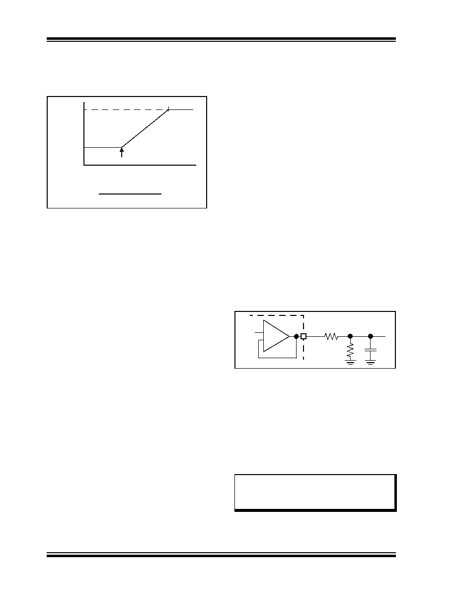
Figure 4-5 shows an example of the slew rate of the
VOUT pin. The slew rate can be affected by the
characteristics of the circuit connected to the VOUT pin.
FIGURE 4-5:
VOUT pin Slew Rate.
4.4.4
SMALL CAPACITIVE LOAD
With a small capacitive load, the output buffer’s current
is not affected by the capacitive load (CL). However, the
VOUT pin’s voltage is not a step transition from one
output value (wiper code value) to the next output
value. The change of the VOUT voltage is limited by the
output buffer’s characteristics, so the VOUT pin voltage
will have a slope from the old voltage to the new
voltage. This slope is fixed for the output buffer, and is
referred to as the buffer slew rate (SRBUF).
4.4.5
LARGE CAPACITIVE LOAD
With a larger capacitive load, the slew rate is deter-
mined by two factors:
The output buffer’s short circuit current (ISC)
The VOUT pin’s external load
IOUT cannot exceed the output buffer’s short circuit
current (ISC) which fixes the output buffer slew rate
(SRBUF). The voltage on the capacitive load (CL), VCL,
changes at a rate proportional to IOUT, which fixes a
capacitive load slew rate (SRCL).
So the VCL voltage slew rate is limited to the slower of
the output buffer’s internally set slew rate (SRBUF) and
the capacitive load slew rate (SRCL).
4.4.6
DRIVING RESISTIVE AND
CAPACITIVE LOADS
The VOUT pin can drive up to 100 pF of capacitive load
in parallel with a 5 k
Ω resistive load (to meet electrical
Resistive Load.
VOUT drops slowly as the load resistance decreases
after about 3.5 k
Ω. It is recommended to use a load
with RL greater than 5 kΩ.
Driving large capacitive loads can cause stability
problems for voltage feedback op amps. As the load
capacitance increases, the feedback loop’s phase
margin decreases and the closed-loop bandwidth is
reduced. This produces gain peaking in the frequency
response with overshoot and ringing in the step
response. That is, since the VOUT pin’s voltage does
not quickly follow the buffer’s input voltage (due to the
large capacitive load), the output buffer will overshoot
the desired target voltage. Once the driver detects this
overshoot, it compensates by forcing it to a voltage
below the target. This causes voltage ringing on the
VOUT pin.
So, when driving large capacitive loads with the output
buffer, a small series resistor (RISO) at the output (see
Figure 4-6) improves the output buffer’s stability
(feedback loop’s phase margin) by making the output
load resistive at higher frequencies. The bandwidth will
be generally lower than the bandwidth with no
capacitive load.
FIGURE 4-6:
Circuit to Stabilize Output
Buffer for Large Capacitive Loads (CL).
The RISO resistor value for your circuit needs to be
selected. The resulting frequency response peaking
and step response overshoot for this RISO resistor
value should be verified on the bench. Modify the
RISO’s resistance value until the output characteristics
meet your requirements.
A method to evaluate the system’s performance is to
inject a step voltage on the VREF pin and observe the
VOUT pin’s characteristics.
Time
Slew Rate =
Wiper = A
V
OUT
VOUT(A)
VOUT(B)
Wiper = B
| VOUT(B) - VOUT(A) |
ΔT
Note:
Additional insight into circuit design for
driving capacitive loads can be found in
AN884 “Driving Capacitive Loads With Op
Amps” (DS00884).
VOUT
Op
Amp
VW
CL
RISO
RL
VCL
相关PDF资料 |
PDF描述 |
|---|---|
| SLP471M200E1P3 | CAP ALUM 470UF 200V 20% SNAP |
| PCX1H330MCL1GS | CAP ALUM 33UF 50V 20% SMD |
| R-725.0D | CONV DC/DC 2A 6.5-28VIN 5V |
| SLPX391M250A5P3 | CAP ALUM 390UF 250V 20% SNAP |
| RBM12DCBD | CONN EDGECARD 24POS R/A .156 SLD |
相关代理商/技术参数 |
参数描述 |
|---|---|
| ADM00333 | 功能描述:开发板和工具包 - PIC / DSPIC PIC18F87J72 Evaluation Board RoHS:否 制造商:Microchip Technology 产品:Starter Kits 工具用于评估:chipKIT 核心:Uno32 接口类型: 工作电源电压: |
| ADM00344 | 功能描述:电源管理IC开发工具 RE46C190 Demo Board RoHS:否 制造商:Maxim Integrated 产品:Evaluation Kits 类型:Battery Management 工具用于评估:MAX17710GB 输入电压: 输出电压:1.8 V |
| ADM00345 | 功能描述:电源管理IC开发工具 3-Phase BLDC Snsrlss Fan Cntrllr RoHS:否 制造商:Maxim Integrated 产品:Evaluation Kits 类型:Battery Management 工具用于评估:MAX17710GB 输入电压: 输出电压:1.8 V |
| ADM00352 | 功能描述:电源管理IC开发工具 MCP16301 600mA Demo Board RoHS:否 制造商:Maxim Integrated 产品:Evaluation Kits 类型:Battery Management 工具用于评估:MAX17710GB 输入电压: 输出电压:1.8 V |
| ADM00360 | 功能描述:电源管理IC开发工具 MCP16301 300mA D2PAK Footprint Demo Board RoHS:否 制造商:Maxim Integrated 产品:Evaluation Kits 类型:Battery Management 工具用于评估:MAX17710GB 输入电压: 输出电压:1.8 V |
发布紧急采购,3分钟左右您将得到回复。