- 您现在的位置:买卖IC网 > PDF目录17099 > ADM00317 (Microchip Technology)BOARD DAUGHTER MCP4706/16/26 PDF资料下载
参数资料
| 型号: | ADM00317 |
| 厂商: | Microchip Technology |
| 文件页数: | 69/86页 |
| 文件大小: | 0K |
| 描述: | BOARD DAUGHTER MCP4706/16/26 |
| 标准包装: | 1 |
| DAC 的数量: | 3 个,每 IC 1 个 |
| 位数: | 8,10,12 |
| 设置时间: | 6µs |
| DAC 型: | 电压 |
| 已供物品: | 子板 |
| 已用 IC / 零件: | MCP4706,MCP4716,MCP4726 |
第1页第2页第3页第4页第5页第6页第7页第8页第9页第10页第11页第12页第13页第14页第15页第16页第17页第18页第19页第20页第21页第22页第23页第24页第25页第26页第27页第28页第29页第30页第31页第32页第33页第34页第35页第36页第37页第38页第39页第40页第41页第42页第43页第44页第45页第46页第47页第48页第49页第50页第51页第52页第53页第54页第55页第56页第57页第58页第59页第60页第61页第62页第63页第64页第65页第66页第67页第68页当前第69页第70页第71页第72页第73页第74页第75页第76页第77页第78页第79页第80页第81页第82页第83页第84页第85页第86页
2011-2012 Microchip Technology Inc.
DS22272C-page 71
MCP4706/4716/4726
8.10
Design Considerations
In the design of a system with the MCP4706/4716/4726
devices, the following considerations should be taken
into account:
8.10.1
POWER SUPPLY
CONSIDERATIONS
The typical application will require a bypass capacitor
in order to filter high-frequency noise, which can be
induced onto the power supply's traces. The bypass
capacitor helps to minimize the effect of these noise
sources on signal integrity. Figure 8-10 illustrates an
appropriate bypass strategy.
In this example, the recommended bypass capacitor
value is 0.1 F. This capacitor should be placed as
close (within 4 mm) to the device power pin (VDD) as
possible.
The power source supplying these devices should be
as clean as possible. If the application circuit has
separate digital and analog power supplies, VDD and
VSS should reside on the analog plane.
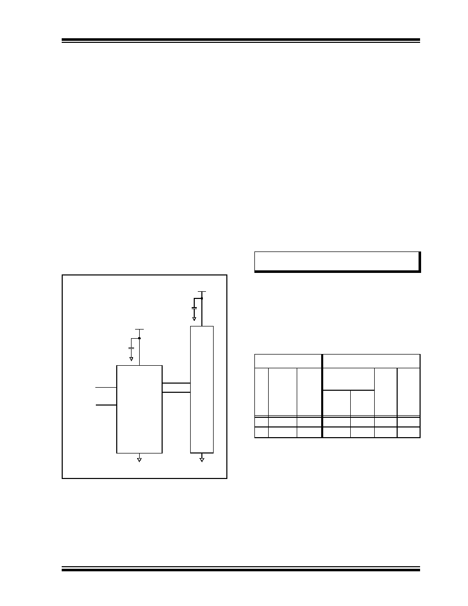
FIGURE 8-10:
Typical Microcontroller
Connections.
8.10.2
LAYOUT CONSIDERATIONS
Several layout considerations may be applicable to
your application. These may include:
8.10.2.1
Noise
Inductively-coupled AC transients and digital switching
noise can degrade the input and output signal integrity,
potentially masking the MCP47X6’s performance.
Careful board layout minimizes these effects and
increases the Signal-to-Noise Ratio (SNR). Multi-layer
boards
utilizing a low-inductance ground plane,
isolated inputs, isolated outputs and proper decoupling
are critical to achieving the performance that the silicon
is
capable
of
providing.
Particularly
harsh
environments may require shielding of critical signals.
Separate digital and analog ground planes are
recommended. In this case, the VSS pin and the ground
pins of the VDD capacitors should be terminated to the
analog ground plane.
8.10.2.2
PCB Area Requirements
In some applications, PCB area is a criteria for device
selection.
shows
the
typical
package
dimensions and area for the different package options.
The table also shows the relative area factor compared
to the smallest area. For space critical applications, the
DFN package would be the suggested package.
VDD
VSS
MCP
47X
6
0.1 F
PIC
Mi
croco
n
trolle
r
0.1 F
SCL
VOUT
VREF
SDA
Note:
Breadboards and wire-wrapped boards
are not recommended.
TABLE 8-2:
PACKAGE FOOTPRINT (1)
Package
Package Footprint
Pins
Type
Code
Dimensions
(mm)
Ar
e
a
(m
m
2
)
Re
la
tiv
e
Are
a
Length Width
6
SOT-23
CH
2.90
2.70
7.83
1.96
6
DFN
MAY
2.00
4.00
1
Note 1: Does not include recommended land
pattern
dimensions.
Dimensions
are
typical values.
相关PDF资料 |
PDF描述 |
|---|---|
| SLP471M200E1P3 | CAP ALUM 470UF 200V 20% SNAP |
| PCX1H330MCL1GS | CAP ALUM 33UF 50V 20% SMD |
| R-725.0D | CONV DC/DC 2A 6.5-28VIN 5V |
| SLPX391M250A5P3 | CAP ALUM 390UF 250V 20% SNAP |
| RBM12DCBD | CONN EDGECARD 24POS R/A .156 SLD |
相关代理商/技术参数 |
参数描述 |
|---|---|
| ADM00333 | 功能描述:开发板和工具包 - PIC / DSPIC PIC18F87J72 Evaluation Board RoHS:否 制造商:Microchip Technology 产品:Starter Kits 工具用于评估:chipKIT 核心:Uno32 接口类型: 工作电源电压: |
| ADM00344 | 功能描述:电源管理IC开发工具 RE46C190 Demo Board RoHS:否 制造商:Maxim Integrated 产品:Evaluation Kits 类型:Battery Management 工具用于评估:MAX17710GB 输入电压: 输出电压:1.8 V |
| ADM00345 | 功能描述:电源管理IC开发工具 3-Phase BLDC Snsrlss Fan Cntrllr RoHS:否 制造商:Maxim Integrated 产品:Evaluation Kits 类型:Battery Management 工具用于评估:MAX17710GB 输入电压: 输出电压:1.8 V |
| ADM00352 | 功能描述:电源管理IC开发工具 MCP16301 600mA Demo Board RoHS:否 制造商:Maxim Integrated 产品:Evaluation Kits 类型:Battery Management 工具用于评估:MAX17710GB 输入电压: 输出电压:1.8 V |
| ADM00360 | 功能描述:电源管理IC开发工具 MCP16301 300mA D2PAK Footprint Demo Board RoHS:否 制造商:Maxim Integrated 产品:Evaluation Kits 类型:Battery Management 工具用于评估:MAX17710GB 输入电压: 输出电压:1.8 V |
发布紧急采购,3分钟左右您将得到回复。