- 您现在的位置:买卖IC网 > PDF目录20428 > ADM00427 (Microchip Technology)BOARD EVALUATION MCP16323 PDF资料下载
参数资料
| 型号: | ADM00427 |
| 厂商: | Microchip Technology |
| 文件页数: | 21/32页 |
| 文件大小: | 0K |
| 描述: | BOARD EVALUATION MCP16323 |
| 标准包装: | 1 |
| 主要目的: | DC/DC,步降 |
| 输出及类型: | 1,非隔离 |
| 输出电压: | 3V |
| 电流 - 输出: | 3A |
| 输入电压: | 6 ~ 18 V |
| 稳压器拓扑结构: | 降压 |
| 频率 - 开关: | 1MHz |
| 板类型: | 完全填充 |
| 已供物品: | 板 |
| 已用 IC / 零件: | MCP16323 |
第1页第2页第3页第4页第5页第6页第7页第8页第9页第10页第11页第12页第13页第14页第15页第16页第17页第18页第19页第20页当前第21页第22页第23页第24页第25页第26页第27页第28页第29页第30页第31页第32页
�� �
�
�MCP16323�
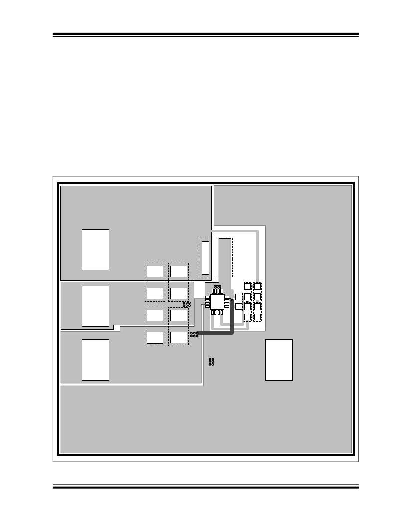
�5.0.9� PCB� LAYOUT� INFORMATION�
�Good� printed� circuit� board� layout� techniques� are�
�important� to� any� switching� circuitry,� and� switching�
�power� supplies� are� no� different.� When� wiring� the�
�switching� high-current� paths,� short� and� wide� traces�
�should� be� used.� Therefore,� it� is� important� that� the� input�
�and� output� capacitors� be� placed� as� close� as� possible� to�
�the� MCP16323� to� minimize� the� loop� area.�
�The� feedback� resistors� and� feedback� signal� should� be�
�routed� away� from� the� switching� node� and� the� switching�
�current� loop.� When� possible,� ground� planes� and� traces�
�should� be� used� to� help� shield� the� feedback� signal� and�
�minimize� noise� and� magnetic� interference.�
�A� good� MCP16323� layout� starts� with� C� IN� placement.�
�C� IN� supplies� current� to� the� input� of� the� circuit� when� the�
�switch� is� turned� on.� In� addition� to� supplying� high-�
�frequency� switch� current,� C� IN� also� provides� a� stable�
�voltage� source� for� the� internal� MCP16323� circuitry.�
�Unstable� PWM� operation� can� result� if� there� are�
�excessive� transients� or� ringing� on� the� V� IN� pin� of� the�
�MCP16323� device.� In� Figure� 5-1� ,� C� IN� is� placed� close� to�
�the� V� IN� pins.� A� ground� plane� on� the� bottom� of� the� board�
�provides� a� low� resistive� and� low� inductive� path� for� the�
�return� current.� The� next� priority� in� placement� is� the�
�freewheeling� current� loop� formed� by� C� OUT� and� L� while�
�strategically� placing� the� C� OUT� return� close� to� C� IN�
�return.� Next,� C� BOOST� should� be� placed� between� the�
�boost� pin� and� the� switch� node� pin.� This� leaves� space�
�close� to� the� MCP16323� V� FB� pin� to� place� R� TOP� and�
�R� BOT� .� R� TOP� and� R� BOT� are� routed� away� from� the� switch�
�node� so� noise� is� not� coupled� into� the� high-impedance�
�V� FB� input.�
�Top� layer� is� made�
�with� 2� oz� copper�
�The� 2� middle�
�layers� are� made�
�V� OUT�
�C� OUT�
�C� OUT�
�L�
�with� 1� oz� copper�
�and� connected� to�
�V� IN� and� GND�
�GND�
�R� PG�
�C� BOOST�
�10� Ω�
�MCP16323�
�Trace� on�
�R� BOT�
�R� TOP�
�V� IN�
�C� IN�
�C� IN�
�bottom� layer�
�GND�
�Bottom� layer� is� a� 2� oz�
�copper� ground� plane�
�Board� Dimensions�
�are� 2.5"� by� 2.5"�
�FIGURE� 5-1:�
�Recommended� Layout.�
�?� 2011� Microchip� Technology� Inc.�
�DS22284A-page� 21�
�相关PDF资料 |
PDF描述 |
|---|---|
| 17PY-Z053-99VS | MOTOR STEP UNI .9DEG 42MM 24V DL |
| ESA06DTMD | CONN EDGECARD 12POS R/A .125 SLD |
| T95Y686M004CSAL | CAP TANT 68UF 4V 20% 2910 |
| MKP1V240RLG | SIDAC BIDIR 0.9A 240V DO-41 |
| AT45DB081B-CNU-2.5 | IC FLASH 8MBIT 20MHZ 8CASON |
相关代理商/技术参数 |
参数描述 |
|---|---|
| ADM00433 | 功能描述:MCP16301 - DC/DC, Step Down 1, Non-Isolated Outputs Evaluation Board 制造商:microchip technology 系列:- 零件状态:有效 主要用途:DC/DC,步降 输出和类型:1,非隔离 功率 - 输出:- 电压 - 输出:5V 电流 - 输出:600mA 电压 - 输入:6 V ~ 30 V 稳压器拓扑:降压 频率 - 开关:- 板类型:完全填充 所含物品:板 使用的 IC/零件:MCP16301 标准包装:1 |
| ADM00434 | 制造商:Microchip Technology Inc 功能描述:MCP19035 300 KHZ SYNCHRONOUS BUCK CONTROLLER EVALUATION BOAR - Boxed Product (Development Kits) 制造商:Microchip Technology Inc 功能描述:BOARD EVAL FOR MCP19035 制造商:Microchip Technology Inc 功能描述:MCP19035 300 kHz Evaluation Board |
| ADM00435 | 功能描述:MCP1643 1, Non-Isolated Output LED Driver Evaluation Board 制造商:microchip technology 系列:- 零件状态:有效 电流 - 输出/通道:25mA,50mA,75mA,或 100mA 输出和类型:1,非隔离 电压 - 输出:- 特性:- 电压 - 输入:0.35 V ~ 2.5 V 所含物品:板 使用的 IC/零件:MCP1643 标准包装:1 |
| ADM00443 | 功能描述:MCP6421 1 - Single Channels per IC General Purpose Amplifier Evaluation Board 制造商:microchip technology 系列:- 零件状态:有效 每 IC 通道数:1 - 单 放大器类型:通用 输出类型:单端,满摆幅 压摆率:0.05 V/μs -3db 带宽:- 电流 - 输出/通道:22mA 工作温度:-40°C ~ 125°C 电流 - 电源(主 IC):4.4μA 电压 - 电源,单/双(±):1.8 V ~ 5.5 V,±0.9 V ~ 2.75 V 板类型:完全填充 所含物品:板 使用的 IC/零件:MCP6421 标准包装:1 |
| ADM00445 | 制造商:Microchip Technology Inc 功能描述:MCP19035 600KHZ EVALUATION BOARD - Boxed Product (Development Kits) 制造商:Microchip Technology Inc 功能描述:BOARD EVAL ANALOG MCP19035 制造商:Microchip Technology Inc 功能描述:MCP19035 600KHz Evaluation Board, DEVTOOL - Analog |
发布紧急采购,3分钟左右您将得到回复。