- 您现在的位置:买卖IC网 > PDF目录22035 > ADM1026JST-REEL (ON Semiconductor)IC CNTRL SYS REF/EEPROM 48LQFP PDF资料下载
参数资料
| 型号: | ADM1026JST-REEL |
| 厂商: | ON Semiconductor |
| 文件页数: | 11/55页 |
| 文件大小: | 0K |
| 描述: | IC CNTRL SYS REF/EEPROM 48LQFP |
| 产品变化通告: | MFG CHG Notification ADI to ON Semi Product Obsolescence 30/Sept/2009 |
| 标准包装: | 2,000 |
| 功能: | 硬件监控器 |
| 传感器类型: | 内部和外部 |
| 感应温度: | 0°C ~ 100°C |
| 精确度: | ±3°C(最小值) |
| 拓扑: | ADC,比较器,多路复用器,寄存器库 |
| 输出类型: | SMBus? |
| 输出警报: | 无 |
| 输出风扇: | 是 |
| 电源电压: | 3 V ~ 5.5 V |
| 工作温度: | 0°C ~ 100°C |
| 安装类型: | 表面贴装 |
| 封装/外壳: | 48-LQFP |
| 供应商设备封装: | 48-LQFP(7x7) |
| 包装: | 带卷 (TR) |
第1页第2页第3页第4页第5页第6页第7页第8页第9页第10页当前第11页第12页第13页第14页第15页第16页第17页第18页第19页第20页第21页第22页第23页第24页第25页第26页第27页第28页第29页第30页第31页第32页第33页第34页第35页第36页第37页第38页第39页第40页第41页第42页第43页第44页第45页第46页第47页第48页第49页第50页第51页第52页第53页第54页第55页
�� �
�
�ADM1026�
�ADM1026� is� powered� down,� unlike� the� data� in� the� volatile�
�registers.� Although� referred� to� as� read-only� memory,� the�
�EEPROM� can� be� written� to� (as� well� as� read� from)� via� the�
�serial� bus� in� exactly� the� same� way� as� the� other� registers.� The�
�main� differences� between� the� EEPROM� and� other� registers�
�are:�
�?� An� EEPROM� location� must� be� blank� before� it� can� be�
�written� to.� If� it� contains� data,� it� must� first� be� erased.�
�?� Writing� to� EEPROM� is� slower� than� writing� to� RAM.�
�?� Writing� to� the� EEPROM� should� be� restricted� because�
�its� typical� cycle� life� is� 100,000� write� operations,� due� to�
�the� usual� EEPROM� wear-out� mechanisms.�
�Serial� Bus� Interface�
�Control� of� the� ADM1026� is� carried� out� via� the� serial�
�system� management� bus� (SMBus).� The� ADM1026� is�
�connected� to� this� bus� as� a� slave� device,� under� the� control� of�
�a� master� device.�
�The� ADM1026� has� a� 7-bit� serial� bus� slave� address.� When�
�the� device� is� powered� on,� it� does� so� with� a� default� serial� bus�
�address.� The� 5� MSBs� of� the� address� are� set� to� 01011,� and� the�
�2� LSBs� are� determined� by� the� logical� states� of� Pin� 15�
�ADD/NTESTOUT.� This� pin� is� a� three-state� input� that� can� be�
�grounded,� connected� to� V� CC� ,� or� left� open-circuit� to� give�
�three� different� addresses.�
�The� EEPROM� in� the� ADM1026� has� been� qualified� for�
�two� key� EEPROM� memory� characteristics:� memory� cycling�
�Table� 6.� ADDRESS� PIN� TRUTH� TABLE�
�ADD� Pin� A1�
�A0�
�endurance� and� memory� data� retention.�
�Endurance� qualifies� the� ability� of� the� EEPROM� to� be�
�cycled� through� many� program,� read,� and� erase� cycles.� In� real�
�terms,� a� single� endurance� cycle� is� composed� of� four�
�GND�
�No� Connect�
�V� CC�
�0�
�1�
�0�
�0�
�0�
�1�
�independent,� sequential� events,� as� follows:�
�1.� Initial� page� erase� sequence�
�2.� Read/verify� sequence�
�3.� Program� sequence�
�4.� Second� read/verify� sequence�
�In� reliability� qualification,� every� byte� is� cycled� from� 00h�
�to� FFh� until� a� first� fail� is� recorded,� signifying� the� endurance�
�limit� of� the� EEPROM� memory.�
�Retention� quantifies� the� ability� of� the� memory� to� retain� its�
�programmed� data� over� time.� The� EEPROM� in� the� ADM1026�
�has� been� qualified� in� accordance� with� the� formal� JEDEC�
�Retention� Lifetime� Specification� (A117)� at� a� specific� junction�
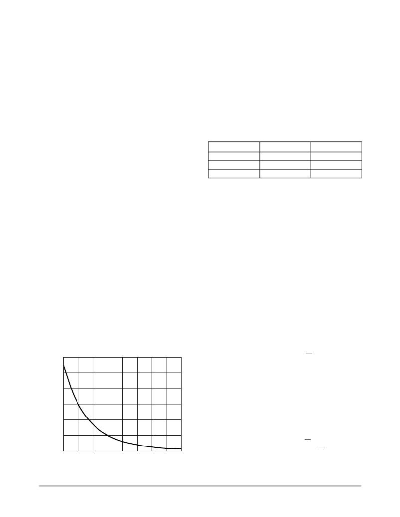
�temperature� (T� J� =� 55� ?� C)� to� guarantee� a� minimum� of� 10� years�
�retention� time.� As� part� of� this� qualification� procedure,� the�
�EEPROM� memory� is� cycled� to� its� specified� endurance� limit�
�described� above� before� data� retention� is� characterized.� This�
�means� that� the� EEPROM� memory� is� guaranteed� to� retain� its�
�data� for� its� full� specified� retention� lifetime� every� time� the�
�EEPROM� is� reprogrammed.� Note� that� retention� lifetime�
�based� on� an� activation� energy� of� 0.6� V� derates� with� T� J� ,� as�
�shown� in� Figure� 15.�
�300�
�250�
�200�
�150�
�100�
�50�
�If� ADD� is� left� open-circuit,� the� default� address� is� 0101110�
�(5Ch).� ADD� is� sampled� only� at� powerup� on� the� first� valid�
�SMBus� transaction,� so� any� changes� made� while� the� power�
�is� on� (and� the� address� is� locked)� have� no� effect.�
�The� facility� to� make� hardwired� changes� to� device�
�addresses� allows� the� user� to� avoid� conflicts� with� other�
�devices� sharing� the� same� serial� bus,� for� example� if� more� than�
�one� ADM1026� is� used� in� a� system.�
�General� SMBus� Timing�
�Figure� 16� and� Figure� 17� show� timing� diagrams� for� general�
�read� and� write� operations� using� the� SMBus.� The� SMBus�
�specification� defines� specific� conditions� for� different� types�
�of� read� and� write� operations,� which� are� discussed� later� in� this�
�section.� The� general� SMBus� protocol� *� operates� as� follows:�
�1.� The� master� initiates� data� transfer� by� establishing� a�
�start� condition,� defined� as� a� high-to-low� transition�
�on� the� serial� data� line� (SDA)� while� the� serial� clock�
�line� SCL� remains� high.� This� indicates� that� a� data�
�stream� follows.� All� slave� peripherals� connected� to�
�the� serial� bus� respond� to� the� start� condition� and�
�shift� in� the� next� 8� bits,� consisting� of� a� 7-bit� slave�
�address� (MSB� first)� and� an� R/W� bit,� which�
�determine� the� direction� of� the� data� transfer,� that� is,�
�whether� data� is� written� to� or� read� from� the� slave�
�device� (0� =� write,� 1� =� read).�
�The� peripheral� whose� address� corresponds� to� the�
�trans-mitted� address� responds� by� pulling� the� data�
�line� low� during� the� low� period� before� the� ninth�
�clock� pulse,� known� as� the� acknowledge� bit,� and�
�holding� it� low� during� the� high� period� of� this� clock�
�pulse.� All� other� devices� on� the� bus� remain� idle�
�while� the� selected� device� waits� for� data� to� be� read�
�from� or� written� to� it.� If� the� R/W� bit� is� 0,� the� master�
�0�
�40�
�50�
�60� 70� 80� 90� 100�
�JUNCTION� TEMPERATURE� (� 5� C)�
�110�
�120�
�writes� to� the� slave� device.� If� the� R/W� bit� is� 1,� the�
�master� reads� from� the� slave� device.�
�Figure� 15.� Typical� EEPROM� Memory� Retention�
�http://onsemi.com�
�11�
�相关PDF资料 |
PDF描述 |
|---|---|
| AGLN020V2-CSG81 | IC FPGA 20K 1.2-1.5V CSP81 |
| ADM1026JST | IC CNTRL SYS REF/EEPROM 48LQFP |
| LQG15HSR22J02D | INDUCTOR 220NH 120MA 0402 |
| GCC10DCSN | CONN EDGECARD 20POS DIP .100 SLD |
| VJ1206Y122KBAAT4X | CAP CER 1200PF 50V 10% X7R 1206 |
相关代理商/技术参数 |
参数描述 |
|---|---|
| ADM1026JST-REEL7 | 功能描述:IC CNTRL SYS REF/EEPROM 48LQFP RoHS:否 类别:集成电路 (IC) >> PMIC - 热管理 系列:- 标准包装:1 系列:- 功能:温度监控系统(传感器) 传感器类型:内部和外部 感应温度:-40°C ~ 125°C,外部传感器 精确度:±2.5°C 本地(最大值),±5°C 远程(最大值) 拓扑:ADC,比较器,寄存器库 输出类型:2 线 SMBus? 输出警报:无 输出风扇:无 电源电压:2.7 V ~ 5.5 V 工作温度:-40°C ~ 125°C 安装类型:表面贴装 封装/外壳:SOT-23-8 供应商设备封装:SOT-23-8 包装:Digi-Reel® 其它名称:296-22675-6 |
| ADM1026JSTZ | 功能描述:PMIC 解决方案 HI INT SYS MONITR IC RoHS:否 制造商:Texas Instruments 安装风格:SMD/SMT 封装 / 箱体:QFN-24 封装:Reel |
| ADM1026JSTZ-R7 | 功能描述:PMIC 解决方案 HI INT SYS MONITR IC RoHS:否 制造商:Texas Instruments 安装风格:SMD/SMT 封装 / 箱体:QFN-24 封装:Reel |
| ADM1026JSTZ-REEL | 功能描述:板上安装温度传感器 HI INT SYS MONITR IC RoHS:否 制造商:Omron Electronics 输出类型:Digital 配置: 准确性:+/- 1.5 C, +/- 3 C 温度阈值: 数字输出 - 总线接口:2-Wire, I2C, SMBus 电源电压-最大:5.5 V 电源电压-最小:4.5 V 最大工作温度:+ 50 C 最小工作温度:0 C 关闭: 安装风格: 封装 / 箱体: 设备功能:Temperature and Humidity Sensor |
| ADM1026JSTZ-REEL7 | 制造商:Analog Devices 功能描述:IC SYSTEM MONITOR 制造商:ON Semiconductor 功能描述:IC SYSTEM MONITOR |
发布紧急采购,3分钟左右您将得到回复。