- 您现在的位置:买卖IC网 > PDF目录16319 > ADM8697ARWZ (Analog Devices Inc)IC SUPERVSR MPU ADJ/RESET 16SOIC PDF资料下载
参数资料
| 型号: | ADM8697ARWZ |
| 厂商: | Analog Devices Inc |
| 文件页数: | 10/13页 |
| 文件大小: | 0K |
| 描述: | IC SUPERVSR MPU ADJ/RESET 16SOIC |
| 标准包装: | 47 |
| 类型: | 备用电池电路 |
| 监视电压数目: | 1 |
| 输出: | 推挽式,推挽式 |
| 复位: | 高有效/低有效 |
| 复位超时: | 最小为 35 ms |
| 电压 - 阀值: | 1.3V |
| 工作温度: | -40°C ~ 85°C |
| 安装类型: | 表面贴装 |
| 封装/外壳: | 16-SOIC(0.295",7.50mm 宽) |
| 供应商设备封装: | 16-SOIC W |
| 包装: | 管件 |
�� �
�
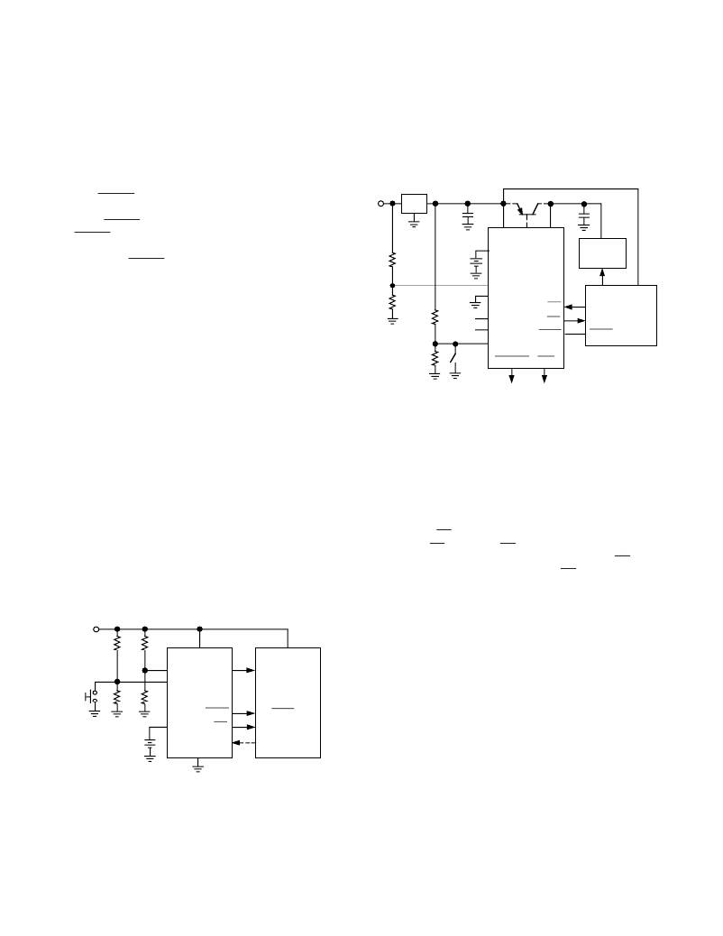
�ADM8696/ADM8697�
�TYPICAL� APPLICATIONS�
�ADM8696�
�Figure� 18� shows� the� ADM8696� in� a� typical� power� monitoring,�
�battery� backup� application.� V� OUT� powers� the� CMOS� RAM.�
�Under� normal� operating� conditions� with� V� CC� present,� V� OUT� is�
�internally� connected� to� V� CC� .� If� a� power� failure� occurs,� V� CC� will�
�decay� and� V� OUT� will� be� switched� to� V� BATT� ,� thereby� maintaining�
�Figure� 18b� shows� a� similar� application� for� the� ADM8696� but� in�
�this� case� the� PFI� input� monitors� the� unregulated� input� to� the�
�7805� voltage� regulator.� This� gives� an� earlier� warning� of� an� im-�
�pending� power� failure.� It� is� useful� with� processors� operating� at�
�low� speeds� or� where� there� are� a� significant� number� of� house-�
�keeping� tasks� to� be� completed� before� the� power� is� lost.�
�power� for� the� CMOS� RAM.�
�Power� Fail� RESET�
�The� V� CC� power� supply� is� also� monitored� by� the� Low� Line� In-�
�INPUT�
�POWER�
�7805�
�0.1� μ� F�
�0.1� μ� F�
�PFO�
�RESET�
�put,� LL� IN� .� A� RESET� pulse� is� generated� when� LL� IN� falls� below�
�1.3� V.� RESET� will� remain� low� for� 50� ms� after� LL� IN� returns�
�above� 1.3� V.� This� allows� for� a� power-on� reset� and� prevents� re-�
�peated� toggling� of� RESET� if� the� V� CC� power� supply� is� unstable.�
�Resistors� R3� and� R4� should� be� chosen� to� give� the� desired� V� CC�
�reset� threshold.�
�Watchdog� Timer�
�The� Watchdog� Timer� Input� (WDI)� monitors� an� I/O� line� from�
�the� μ� P� system.� This� line� must� be� toggled� once� every� 1.6� s� to�
�verify� correct� software� execution.� Failure� to� toggle� the� line� indi-�
�cates� that� the� μ� P� system� is� not� correctly� executing� its� program�
�R1�
�R2�
�R3�
�R4�
�3V�
�BATTERY�
�NC�
�RESET�
�V� CC� BATT� V� OUT�
�ON�
�V� BATT�
�ADM8696�
�PFI�
�GND�
�WDI�
�OSC� IN�
�OSC� SEL�
�LL� IN�
�LOW� LINE� WDO�
�V� CC�
�CMOS� RAM�
�A0–A15�
�I/O� LINE�
�NMI�
�RESET�
�μ� P�
�POWER�
�μ� P�
�and� may� be� tied� up� in� an� endless� loop.� If� this� happens,� a� reset�
�pulse� is� generated� to� initialize� the� processor.�
�If� the� watchdog� timer� is� not� needed� the� WDI� input� should� be�
�left� floating.�
�Power� Fail� Detector�
�The� Power� Fail� Input,� PFI,� monitors� the� input� power� supply� via�
�a� resistive� divider� network� R1� and� R2.� This� input� is� intended� as�
�an� early� warning� power� fail� input.� The� voltage� on� the� PFI� input�
�is� compared� with� a� precision� 1.3� V� internal� reference.� If� the� in-�
�put� voltage� drops� below� 1.3� V,� a� power� fail� output� (PFO)� signal�
�is� generated.� This� warns� of� an� impending� power� failure� and� may�
�be� used� to� interrupt� the� processor� so� that� the� system� may� be�
�shut� down� in� an� orderly� fashion.� The� resistors� in� the� sensing�
�network� are� ratioed� to� give� the� desired� power� fail� threshold� volt-�
�age� V� T� .� The� threshold� should� be� set� at� a� higher� voltage� than� the�
�RESET� threshold� so� there� is� sufficient� time� available� to� com-�
�plete� the� shutdown� procedure� before� the� processor� is� RESET�
�and� power� is� lost.�
�SYSTEM� STATUS�
�INDICATORS�
�Figure� 18b.� ADM8696� Typical� Application� Circuit� B�
�This� application� also� shows� an� optional� external� transistor� that�
�may� be� used� to� provide� in� excess� of� 100� mA� current� on� V� OUT� .�
�When� V� CC� is� higher� than� V� BATT� ,� the� BATT� ON� output� goes�
�low,� providing� 25� mA� of� base� drive� for� the� external� PNP� transis-�
�tor.� The� maximum� current� available� is� dependent� on� the� power�
�rating� of� the� external� transistor.�
�RAM� Write� Protection�
�The� ADM8697� CE� OUT� line� drives� the� Chip� Select� inputs� of� the�
�CMOS� RAM.� CE� OUT� follows� CE� IN� as� long� as� LL� IN� is� above� the�
�reset� threshold.� If� LL� IN� falls� below� the� reset� threshold,� CE� OUT�
�goes� high,� independent� of� the� logic� level� at� CE� IN� .� This� prevents�
�the� microprocessor� from� writing� erroneous� data� into� RAM� dur-�
�ing� power-up,� power-down,� brownouts� and� momentary� power�
�interruptions.�
�+5V�
�R3�
�R1�
�V� CC�
�μ� P� POWER�
�RESET�
�R4�
�R2�
�PFI� V� OUT�
�LL� IN�
�ADM8696�
�CMOS� RAM�
�POWER�
�μ� P� SYSTEM�
�RESET�
�μ� P� RESET�
�BATTERY�
�+�
�V� BATT�
�GND�
�PFO�
�WDI�
�μ� P� NMI�
�I/O� LINE�
�Figure� 18a.� ADM8696� Typical� Application� Circuit� A�
�–10� –�
�REV. A�
�相关PDF资料 |
PDF描述 |
|---|---|
| GEC28DRAH | CONN EDGECARD 56POS R/A .100 SLD |
| RBC12DRTI-S734 | CONN EDGECARD 24POS DIP .100 SLD |
| ADM8696ARWZ | IC SUPERVSR MPU ADJ/RESET 16SOIC |
| A3AAB-4036G | IDC CABLE- ASC40B/AE40G/ASC40B |
| 2-6754410-5 | CA,XG,MTRJ-SC |
相关代理商/技术参数 |
参数描述 |
|---|---|
| ADM8698 | 制造商:AD 制造商全称:Analog Devices 功能描述:Microprocessor Supervisory Circuits |
| ADM8698AN | 功能描述:IC SUPERVISOR MPU 4.65V 8DIP RoHS:否 类别:集成电路 (IC) >> PMIC - 监控器 系列:- 标准包装:1 系列:- 类型:简单复位/加电复位 监视电压数目:1 输出:开路漏极或开路集电极 复位:高有效 复位超时:- 电压 - 阀值:1.8V 工作温度:-40°C ~ 125°C 安装类型:表面贴装 封装/外壳:6-TSOP(0.059",1.50mm 宽)5 引线 供应商设备封装:5-TSOP 包装:剪切带 (CT) 其它名称:NCP301HSN18T1GOSCT |
| ADM8698ANZ | 功能描述:IC SUPERVISOR MPU 4.65V 8DIP RoHS:是 类别:集成电路 (IC) >> PMIC - 监控器 系列:- 标准包装:1 系列:- 类型:简单复位/加电复位 监视电压数目:1 输出:开路漏极或开路集电极 复位:高有效 复位超时:- 电压 - 阀值:1.8V 工作温度:-40°C ~ 125°C 安装类型:表面贴装 封装/外壳:6-TSOP(0.059",1.50mm 宽)5 引线 供应商设备封装:5-TSOP 包装:剪切带 (CT) 其它名称:NCP301HSN18T1GOSCT |
| ADM8698ARN | 功能描述:IC SUPERVISOR MPU 4.65V 8SOIC RoHS:否 类别:集成电路 (IC) >> PMIC - 监控器 系列:- 标准包装:1 系列:- 类型:简单复位/加电复位 监视电压数目:1 输出:开路漏极或开路集电极 复位:高有效 复位超时:- 电压 - 阀值:1.8V 工作温度:-40°C ~ 125°C 安装类型:表面贴装 封装/外壳:6-TSOP(0.059",1.50mm 宽)5 引线 供应商设备封装:5-TSOP 包装:剪切带 (CT) 其它名称:NCP301HSN18T1GOSCT |
| ADM8698ARN-REEL | 制造商:Analog Devices 功能描述:Processor Supervisor 4.65V 3V to 5.5V 8-Pin SOIC N T/R 制造商:Analog Devices 功能描述:IMPROVED ADM698 - Tape and Reel 制造商:Rochester Electronics LLC 功能描述:IMPROVED ADM698 - Tape and Reel |
发布紧急采购,3分钟左右您将得到回复。