- 您现在的位置:买卖IC网 > PDF目录1989 > ADN2813ACPZ-500RL7 (Analog Devices Inc)IC CLK/DATA REC 1.25GBPS 32LFCSP PDF资料下载
参数资料
| 型号: | ADN2813ACPZ-500RL7 |
| 厂商: | Analog Devices Inc |
| 文件页数: | 14/28页 |
| 文件大小: | 0K |
| 描述: | IC CLK/DATA REC 1.25GBPS 32LFCSP |
| 标准包装: | 500 |
| 类型: | 时钟和数据恢复(CDR),多路复用器 |
| PLL: | 是 |
| 主要目的: | SONET/SDH |
| 输入: | CML |
| 输出: | LVDS |
| 电路数: | 1 |
| 比率 - 输入:输出: | 1:2 |
| 差分 - 输入:输出: | 是/是 |
| 频率 - 最大: | 1.25GHz |
| 电源电压: | 3 V ~ 3.6 V |
| 工作温度: | -40°C ~ 85°C |
| 安装类型: | 表面贴装 |
| 封装/外壳: | 32-VFQFN 裸露焊盘,CSP |
| 供应商设备封装: | 32-LFCSP-VQ(5x5) |
| 包装: | 带卷 (TR) |
第1页第2页第3页第4页第5页第6页第7页第8页第9页第10页第11页第12页第13页当前第14页第15页第16页第17页第18页第19页第20页第21页第22页第23页第24页第25页第26页第27页第28页
ADN2813
Rev. B | Page 21 of 2
8
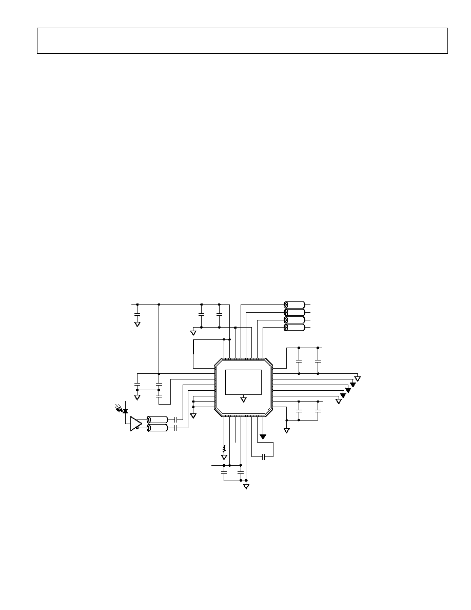
APPLICATIONS INFORMATION
PCB DESIGN GUIDELINES
Proper RF PCB design techniques must be used for optimal
performance.
Power Supply Connections and Ground Planes
Use of one low impedance ground plane is recommended. The
VEE pins should be soldered directly to the ground plane to
reduce series inductance. If the ground plane is an internal
plane and connections to the ground plane are made through
vias, multiple vias can be used in parallel to reduce the series
inductance, especially on Pin 23, which is the ground return for
the output buffers. The exposed pad should be connected to the
GND plane using plugged vias so that solder does not leak
through the vias during reflow.
Use of a 22 μF electrolytic capacitor between VCC and VEE is
recommended at the location where the 3.3 V supply enters the
PCB. When using 0.1 μF and 1 nF ceramic chip capacitors, they
should be placed between the IC power supply VCC and VEE,
as close as possible to the ADN2813 VCC pins.
If connections to the supply and ground are made through
vias, the use of multiple vias in parallel helps to reduce series
inductance, especially on Pin 24, which supplies power to the
high speed CLKOUTP/CLKOUTN and DATAOUTP/
DATAOUTN output buffers. Refer to Figure 24 for the
recommended connections.
By using adjacent power supply and GND planes, excellent high
frequency decoupling can be realized by using close spacing
between the planes. This capacitance is given by
( )
pF
0.88εr A/d
CPLANE =
where:
ε
r
is the dielectric constant of the PCB material.
A is the area of the overlap of power and GND planes (cm2).
d is the separation between planes (mm).
For FR-4, εr = 4.4 mm and 0.25 mm spacing, C ~15 pF/cm2.
50
TRANSMISSION LINES
DATAOUTP
DATAOUTN
CLKOUTP
CLKOUTN
0.1F
22F
1nF
0.1F
0.47F ±20%
>300M
INSULATION RESISTANCE
1nF
0.1F
1nF
+
VCC
50
50
CIN
TIA
VCC
RTH
VCC
NC
C
I2C CONTROLLER
VCC
04
95
1-
0-
0
31
1
VCC
2
VCC
3
VREF
4
NIN
5
PIN
6
SLICEP
7
SLICEN
8
VEE
24
VCC
23
VEE
22
LOS
21
SDA
20
SCK
19
SADDR5
18
VCC
17
VEE
9
T
H
R
A
D
J
1
0
R
E
F
C
L
K
P
1
R
E
F
C
L
K
N
1
2
V
C
1
3
V
E
1
4
C
F
2
1
5
C
F
1
6
L
O
L
3
2
V
C
3
1
V
C
3
0
V
E
2
9
D
A
T
A
O
U
T
P
2
8
D
A
T
A
O
U
T
N
2
7
S
Q
U
E
L
C
H
2
6
C
L
K
O
U
T
P
2
5
C
L
K
O
U
T
N
EXPOSED PAD
TIED OFF TO
VEE PLANE
WITH VIAS
Figure 24. Typical ADN2813 Applications Circuit
相关PDF资料 |
PDF描述 |
|---|---|
| ADN2814ACPZ-500RL7 | IC CLK/DATA REC 675MBPS 32-LFCSP |
| ADN2815ACPZ | IC CLK/DATA REC 1.25GBPS 32LFCSP |
| ADN2816ACPZ-500RL7 | IC CLK/DATA REC 675MBPS 32-LFCSP |
| ADN2817ACPZ-RL7 | IC CLOCK/DATA RECOVERY 32-LFCSP |
| ADN2819ACPZ-CML | IC CLOCK/DATA RECOVERY 48LFCSP |
相关代理商/技术参数 |
参数描述 |
|---|---|
| ADN2813ACPZ-RL7 | 功能描述:IC CLK/DATA REC 1.25GBPS 32LFCSP RoHS:是 类别:集成电路 (IC) >> 时钟/计时 - 专用 系列:- 标准包装:1 系列:- 类型:时钟/频率发生器,多路复用器 PLL:是 主要目的:存储器,RDRAM 输入:晶体 输出:LVCMOS 电路数:1 比率 - 输入:输出:1:2 差分 - 输入:输出:无/是 频率 - 最大:400MHz 电源电压:3 V ~ 3.6 V 工作温度:0°C ~ 85°C 安装类型:表面贴装 封装/外壳:16-TSSOP(0.173",4.40mm 宽) 供应商设备封装:16-TSSOP 包装:Digi-Reel® 其它名称:296-6719-6 |
| ADN2814 | 制造商:Analog Devices 功能描述: |
| ADN2814ACPZ | 功能描述:IC CLOCK/DATA RECOVERY 32LFCSP RoHS:是 类别:集成电路 (IC) >> 时钟/计时 - 专用 系列:- 标准包装:1 系列:- 类型:时钟/频率发生器,多路复用器 PLL:是 主要目的:存储器,RDRAM 输入:晶体 输出:LVCMOS 电路数:1 比率 - 输入:输出:1:2 差分 - 输入:输出:无/是 频率 - 最大:400MHz 电源电压:3 V ~ 3.6 V 工作温度:0°C ~ 85°C 安装类型:表面贴装 封装/外壳:16-TSSOP(0.173",4.40mm 宽) 供应商设备封装:16-TSSOP 包装:Digi-Reel® 其它名称:296-6719-6 |
| ADN2814ACPZ-500RL7 | 功能描述:IC CLK/DATA REC 675MBPS 32-LFCSP RoHS:是 类别:集成电路 (IC) >> 时钟/计时 - 专用 系列:- 标准包装:28 系列:- 类型:时钟/频率发生器 PLL:是 主要目的:Intel CPU 服务器 输入:时钟 输出:LVCMOS 电路数:1 比率 - 输入:输出:3:22 差分 - 输入:输出:无/是 频率 - 最大:400MHz 电源电压:3.135 V ~ 3.465 V 工作温度:0°C ~ 85°C 安装类型:表面贴装 封装/外壳:64-TFSOP (0.240",6.10mm 宽) 供应商设备封装:64-TSSOP 包装:管件 |
| ADN2814ACPZ-RL7 | 功能描述:IC CLK/DATA REC 675MBPS 32-LFCSP RoHS:是 类别:集成电路 (IC) >> 时钟/计时 - 专用 系列:- 标准包装:28 系列:- 类型:时钟/频率发生器 PLL:是 主要目的:Intel CPU 服务器 输入:时钟 输出:LVCMOS 电路数:1 比率 - 输入:输出:3:22 差分 - 输入:输出:无/是 频率 - 最大:400MHz 电源电压:3.135 V ~ 3.465 V 工作温度:0°C ~ 85°C 安装类型:表面贴装 封装/外壳:64-TFSOP (0.240",6.10mm 宽) 供应商设备封装:64-TSSOP 包装:管件 |
发布紧急采购,3分钟左右您将得到回复。