- 您现在的位置:买卖IC网 > PDF目录1989 > ADN2813ACPZ-500RL7 (Analog Devices Inc)IC CLK/DATA REC 1.25GBPS 32LFCSP PDF资料下载
参数资料
| 型号: | ADN2813ACPZ-500RL7 |
| 厂商: | Analog Devices Inc |
| 文件页数: | 4/28页 |
| 文件大小: | 0K |
| 描述: | IC CLK/DATA REC 1.25GBPS 32LFCSP |
| 标准包装: | 500 |
| 类型: | 时钟和数据恢复(CDR),多路复用器 |
| PLL: | 是 |
| 主要目的: | SONET/SDH |
| 输入: | CML |
| 输出: | LVDS |
| 电路数: | 1 |
| 比率 - 输入:输出: | 1:2 |
| 差分 - 输入:输出: | 是/是 |
| 频率 - 最大: | 1.25GHz |
| 电源电压: | 3 V ~ 3.6 V |
| 工作温度: | -40°C ~ 85°C |
| 安装类型: | 表面贴装 |
| 封装/外壳: | 32-VFQFN 裸露焊盘,CSP |
| 供应商设备封装: | 32-LFCSP-VQ(5x5) |
| 包装: | 带卷 (TR) |
第1页第2页第3页当前第4页第5页第6页第7页第8页第9页第10页第11页第12页第13页第14页第15页第16页第17页第18页第19页第20页第21页第22页第23页第24页第25页第26页第27页第28页
ADN2813
Rev. B | Page 12 of
28
TERMINOLOGY
Input Sensitivity and Input Overdrive
Sensitivity and overdrive specifications for the quantizer involve
offset voltage, gain, and noise. The relationship between the
logic output of the quantizer and the analog voltage input is
shown in Figure 12. For sufficiently large positive input voltage,
the output is always Logic 1, and similarly for negative inputs,
the output is always Logic 0. However, the transitions between
output Logic 1 and output Logic 0 are not at precisely defined
input voltage levels but occur over a range of input voltages.
Within this range of input voltages, the output may be either 1
or 0, or it may even fail to attain a valid logic state. The width of
this zone is determined by the input voltage noise of the
quantizer. The center of the zone is the quantizer input offset
voltage. Input overdrive is the magnitude of signal required to
guarantee the correct logic level with 1 × 10¹⁰ confidence level.
04951-0-012
NOISE
OUTPUT
INPUT (V p-p)
OFFSET
OVERDRIVE
SENSITIVITY
(2
× OVERDRIVE)
1
0
Figure 12. Input Sensitivity and Input Overdrive
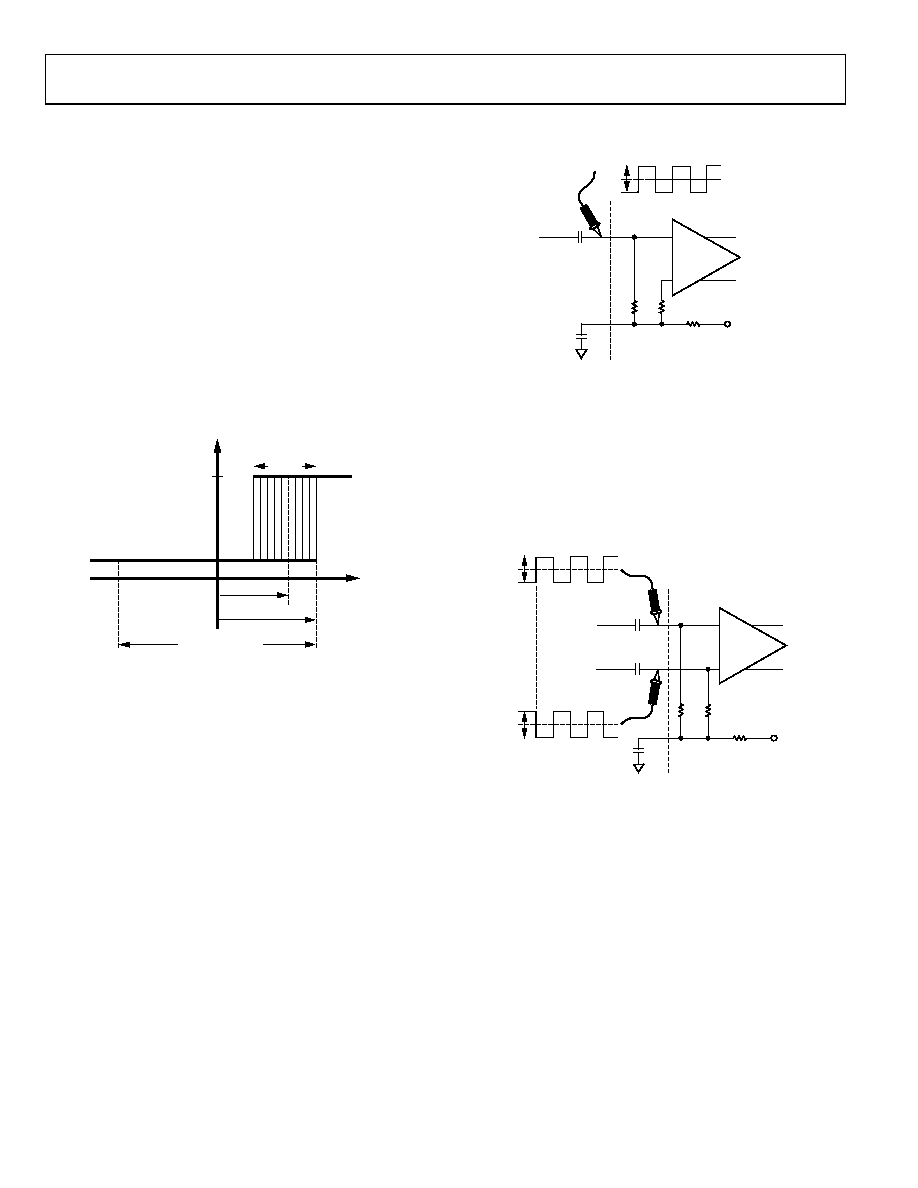
Single-Ended vs. Differential
AC coupling is typically used to drive the inputs to the
quantizer. The inputs are internally dc biased to a common-
mode potential of ~2.5 V. Driving the ADN2813 single-ended
and observing the quantizer input with an oscilloscope probe at
the point indicated in Figure 13 shows a binary signal with an
average value equal to the common-mode potential and
instantaneous values both above and below the average value. It
is convenient to measure the peak-to-peak amplitude of this
signal and call the minimum required value the quantizer
sensitivity. Referring to Figure 13, because both positive and
negative offsets need to be accommodated, the sensitivity is
twice the overdrive. The ADN2813 quantizer typically has
3.3 mV p-p sensitivity.
04951-0-013
SCOPE
PROBE
PIN
50
Ω
3k
Ω
2.5V
50
Ω
VREF
ADN2813
QUANTIZER
+
–
10mV p-p
VREF
Figure 13. Single-Ended Sensitivity Measurement
Driving the ADN2813 differentially (see Figure 14), sensitivity
seems to improve from observing the quantizer input with an
oscilloscope probe. This is an illusion caused by the use of a
single-ended probe. A 5 mV p-p signal appears to drive the
ADN2813 quantizer. However, the single-ended probe
measures only half the signal. The true quantizer input signal is
twice this value, because the other quantizer input is a
complementary signal to the signal being observed.
04951-0-014
SCOPE
PROBE
PIN
50
Ω
3k
Ω
2.5V
50
Ω
VREF
QUANTIZER
+
–
NIN
5mV p-p
VREF
5mV p-p
VREF
Figure 14. Differential Sensitivity Measurement
LOS Response Time
LOS response time is the delay between removal of the input
signal and indication of loss of signal (LOS) at the LOS output,
Pin 22. When the inputs are dc-coupled, the LOS assert time of
the ADN2813 is 500 ns typical and the deassert time is 400 ns
typical. In practice, the time constant produced by the ac
coupling at the quantizer input and the 50 Ω on-chip input
termination determines the LOS response time.
相关PDF资料 |
PDF描述 |
|---|---|
| ADN2814ACPZ-500RL7 | IC CLK/DATA REC 675MBPS 32-LFCSP |
| ADN2815ACPZ | IC CLK/DATA REC 1.25GBPS 32LFCSP |
| ADN2816ACPZ-500RL7 | IC CLK/DATA REC 675MBPS 32-LFCSP |
| ADN2817ACPZ-RL7 | IC CLOCK/DATA RECOVERY 32-LFCSP |
| ADN2819ACPZ-CML | IC CLOCK/DATA RECOVERY 48LFCSP |
相关代理商/技术参数 |
参数描述 |
|---|---|
| ADN2813ACPZ-RL7 | 功能描述:IC CLK/DATA REC 1.25GBPS 32LFCSP RoHS:是 类别:集成电路 (IC) >> 时钟/计时 - 专用 系列:- 标准包装:1 系列:- 类型:时钟/频率发生器,多路复用器 PLL:是 主要目的:存储器,RDRAM 输入:晶体 输出:LVCMOS 电路数:1 比率 - 输入:输出:1:2 差分 - 输入:输出:无/是 频率 - 最大:400MHz 电源电压:3 V ~ 3.6 V 工作温度:0°C ~ 85°C 安装类型:表面贴装 封装/外壳:16-TSSOP(0.173",4.40mm 宽) 供应商设备封装:16-TSSOP 包装:Digi-Reel® 其它名称:296-6719-6 |
| ADN2814 | 制造商:Analog Devices 功能描述: |
| ADN2814ACPZ | 功能描述:IC CLOCK/DATA RECOVERY 32LFCSP RoHS:是 类别:集成电路 (IC) >> 时钟/计时 - 专用 系列:- 标准包装:1 系列:- 类型:时钟/频率发生器,多路复用器 PLL:是 主要目的:存储器,RDRAM 输入:晶体 输出:LVCMOS 电路数:1 比率 - 输入:输出:1:2 差分 - 输入:输出:无/是 频率 - 最大:400MHz 电源电压:3 V ~ 3.6 V 工作温度:0°C ~ 85°C 安装类型:表面贴装 封装/外壳:16-TSSOP(0.173",4.40mm 宽) 供应商设备封装:16-TSSOP 包装:Digi-Reel® 其它名称:296-6719-6 |
| ADN2814ACPZ-500RL7 | 功能描述:IC CLK/DATA REC 675MBPS 32-LFCSP RoHS:是 类别:集成电路 (IC) >> 时钟/计时 - 专用 系列:- 标准包装:28 系列:- 类型:时钟/频率发生器 PLL:是 主要目的:Intel CPU 服务器 输入:时钟 输出:LVCMOS 电路数:1 比率 - 输入:输出:3:22 差分 - 输入:输出:无/是 频率 - 最大:400MHz 电源电压:3.135 V ~ 3.465 V 工作温度:0°C ~ 85°C 安装类型:表面贴装 封装/外壳:64-TFSOP (0.240",6.10mm 宽) 供应商设备封装:64-TSSOP 包装:管件 |
| ADN2814ACPZ-RL7 | 功能描述:IC CLK/DATA REC 675MBPS 32-LFCSP RoHS:是 类别:集成电路 (IC) >> 时钟/计时 - 专用 系列:- 标准包装:28 系列:- 类型:时钟/频率发生器 PLL:是 主要目的:Intel CPU 服务器 输入:时钟 输出:LVCMOS 电路数:1 比率 - 输入:输出:3:22 差分 - 输入:输出:无/是 频率 - 最大:400MHz 电源电压:3.135 V ~ 3.465 V 工作温度:0°C ~ 85°C 安装类型:表面贴装 封装/外壳:64-TFSOP (0.240",6.10mm 宽) 供应商设备封装:64-TSSOP 包装:管件 |
发布紧急采购,3分钟左右您将得到回复。