- 您现在的位置:买卖IC网 > PDF目录1989 > ADN2813ACPZ-500RL7 (Analog Devices Inc)IC CLK/DATA REC 1.25GBPS 32LFCSP PDF资料下载
参数资料
| 型号: | ADN2813ACPZ-500RL7 |
| 厂商: | Analog Devices Inc |
| 文件页数: | 9/28页 |
| 文件大小: | 0K |
| 描述: | IC CLK/DATA REC 1.25GBPS 32LFCSP |
| 标准包装: | 500 |
| 类型: | 时钟和数据恢复(CDR),多路复用器 |
| PLL: | 是 |
| 主要目的: | SONET/SDH |
| 输入: | CML |
| 输出: | LVDS |
| 电路数: | 1 |
| 比率 - 输入:输出: | 1:2 |
| 差分 - 输入:输出: | 是/是 |
| 频率 - 最大: | 1.25GHz |
| 电源电压: | 3 V ~ 3.6 V |
| 工作温度: | -40°C ~ 85°C |
| 安装类型: | 表面贴装 |
| 封装/外壳: | 32-VFQFN 裸露焊盘,CSP |
| 供应商设备封装: | 32-LFCSP-VQ(5x5) |
| 包装: | 带卷 (TR) |
第1页第2页第3页第4页第5页第6页第7页第8页当前第9页第10页第11页第12页第13页第14页第15页第16页第17页第18页第19页第20页第21页第22页第23页第24页第25页第26页第27页第28页
ADN2813
Rev. B | Page 17 of
28
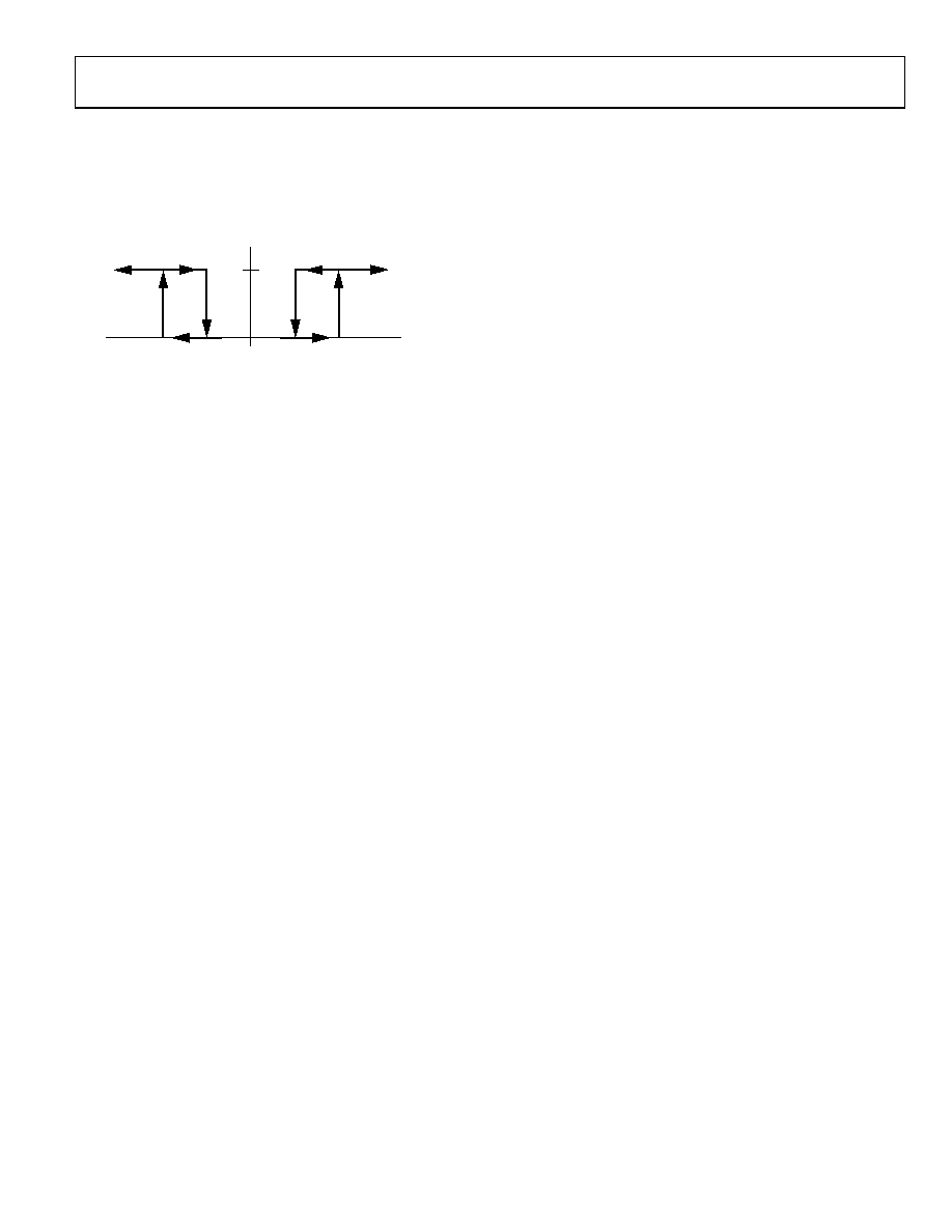
exceeds 1000 ppm (0.1%), the loss-of-lock signal is reasserted
and control returns to the frequency loop, which begins a new
frequency acquisition starting at the lowest point in the VCO
operating range, 10 MHz. The LOL pin remains asserted until
the VCO locks onto a valid input data stream to within 250
ppm frequency error. This hysteresis is shown in Figure 20.
04951-0-020
LOL
0
–250
250
1000
fVCO ERROR
(ppm)
–1000
1
Figure 20. Transfer Function of LOL
LOL Detector Operation Using a Reference Clock
ition aid
e
he
res
h
lements a static LOL feature, which indicates
LOL
e
y
In REFCLK mode, a reference clock is used as an acquis
to lock the ADN2813 VCO. Lock-to-reference mode is enabled
by setting CTRLA[0] to 1. The user also needs to write to
the CTRLA[7:6] and CTRLA[5:2] bits to set the reference
frequency range and the divide ratio of the data rate with
respect to the reference frequency. For more details, see th
Reference Clock (Optional) section. In this mode, the lock
detector monitors the difference in frequency between the
divided down VCO and the divided down reference clock. T
loss-of-lock signal, which appears on Pin 16, LOL, is deasserted
when the VCO is within 250 ppm of the desired frequency. This
enables the D/PLL, which pulls the VCO frequency in the
remaining amount with respect to the input data and acqui
phase lock. Once locked, if the input frequency error exceeds
1000 ppm (0.1%), the loss-of-lock signal is reasserted and
control returns to the frequency loop, which reacquires wit
respect to the reference clock. The LOL pin remains asserted
until the VCO frequency is within 250 ppm of the desired
frequency. This hysteresis is shown in Figure 20.
Static LOL Mode
The ADN2813 imp
if a loss-of-lock condition has ever occurred and remains
asserted, even if the ADN2813 regains lock, until the static
bit is manually reset. The I2C register bit, MISC[4], is the static
LOL bit. If there is ever an occurrence of a loss-of-lock
condition, this bit is internally asserted to logic high. Th
MISC[4] bit remains high even after the ADN2813 has
reacquired lock to a new data rate. This bit can be reset b
writing a 1 followed by 0 to I2C Register Bit CTRLB[6]. Once
reset, the MISC[4] bit remains deasserted until another loss-of-
lock condition occurs.
Writing a 1 to I2C Register Bit CTRLB[7] causes the LOL pin,
Pin 16, to become a static LOL indicator. In this mode, the
LOL pin mirrors the contents of the MISC[4] bit and has
the functionality described in the previous paragraph. The
CTRLB[7] bit defaults to 0. In this mode, the LOL pin operates
in the normal operating mode, that is, it is asserted only when
the ADN2813 is in acquisition mode and deasserts when the
ADN2813 has reacquired lock.
HARMONIC DETECTOR
The ADN2813 provides a harmonic detector, which detects
whether or not the input data has changed to a lower harmonic
of the data rate that the VCO is currently locked onto. For
example, if the input data instantaneously changes from OC-12,
622.08 Mb/s to an OC-3, 155.52 Mb/s bit stream, this could be
perceived as a valid OC-12 bit stream, because the OC-3 data
pattern is exactly 4× slower than the OC-12 pattern. Therefore,
if the change in data rate is instantaneous, a 101 pattern at OC-3
would be perceived by the ADN2813 as a 111100001111 pattern
at OC-12. If the change to a lower harmonic is instantaneous, a
typical CDR could remain locked at the higher data rate.
The ADN2813 implements a harmonic detector that automati-
cally identifies whether or not the input data has switched to a
lower harmonic of the data rate that the VCO is currently
locked onto. When a harmonic is identified, the LOL pin is
asserted and a new frequency acquisition is initiated. The
ADN2813 automatically locks onto the new data rate, and the
LOL pin is deasserted.
However, the harmonic detector does not detect higher
harmonics of the data rate. If the input data rate switches to a
higher harmonic of the data rate, then the VCO is currently
locked onto, the VCO loses lock, the LOL pin is asserted, and a
new frequency acquisition is initiated. The ADN2813
automatically locks onto the new data rate.
The time to detect lock to harmonic is
216 × (Td/ρ)
where:
1/Td is the new data rate. For example, if the data rate is
switched from OC-12 to OC-3, then Td = 1/155.52 MHz.
ρ is the data transition density. Most coding schemes seek to
ensure that ρ = 0.5, for example, PRBS, 8B/10B.
When the ADN2813 is placed in lock-to-reference mode, the
harmonic detector is disabled.
相关PDF资料 |
PDF描述 |
|---|---|
| ADN2814ACPZ-500RL7 | IC CLK/DATA REC 675MBPS 32-LFCSP |
| ADN2815ACPZ | IC CLK/DATA REC 1.25GBPS 32LFCSP |
| ADN2816ACPZ-500RL7 | IC CLK/DATA REC 675MBPS 32-LFCSP |
| ADN2817ACPZ-RL7 | IC CLOCK/DATA RECOVERY 32-LFCSP |
| ADN2819ACPZ-CML | IC CLOCK/DATA RECOVERY 48LFCSP |
相关代理商/技术参数 |
参数描述 |
|---|---|
| ADN2813ACPZ-RL7 | 功能描述:IC CLK/DATA REC 1.25GBPS 32LFCSP RoHS:是 类别:集成电路 (IC) >> 时钟/计时 - 专用 系列:- 标准包装:1 系列:- 类型:时钟/频率发生器,多路复用器 PLL:是 主要目的:存储器,RDRAM 输入:晶体 输出:LVCMOS 电路数:1 比率 - 输入:输出:1:2 差分 - 输入:输出:无/是 频率 - 最大:400MHz 电源电压:3 V ~ 3.6 V 工作温度:0°C ~ 85°C 安装类型:表面贴装 封装/外壳:16-TSSOP(0.173",4.40mm 宽) 供应商设备封装:16-TSSOP 包装:Digi-Reel® 其它名称:296-6719-6 |
| ADN2814 | 制造商:Analog Devices 功能描述: |
| ADN2814ACPZ | 功能描述:IC CLOCK/DATA RECOVERY 32LFCSP RoHS:是 类别:集成电路 (IC) >> 时钟/计时 - 专用 系列:- 标准包装:1 系列:- 类型:时钟/频率发生器,多路复用器 PLL:是 主要目的:存储器,RDRAM 输入:晶体 输出:LVCMOS 电路数:1 比率 - 输入:输出:1:2 差分 - 输入:输出:无/是 频率 - 最大:400MHz 电源电压:3 V ~ 3.6 V 工作温度:0°C ~ 85°C 安装类型:表面贴装 封装/外壳:16-TSSOP(0.173",4.40mm 宽) 供应商设备封装:16-TSSOP 包装:Digi-Reel® 其它名称:296-6719-6 |
| ADN2814ACPZ-500RL7 | 功能描述:IC CLK/DATA REC 675MBPS 32-LFCSP RoHS:是 类别:集成电路 (IC) >> 时钟/计时 - 专用 系列:- 标准包装:28 系列:- 类型:时钟/频率发生器 PLL:是 主要目的:Intel CPU 服务器 输入:时钟 输出:LVCMOS 电路数:1 比率 - 输入:输出:3:22 差分 - 输入:输出:无/是 频率 - 最大:400MHz 电源电压:3.135 V ~ 3.465 V 工作温度:0°C ~ 85°C 安装类型:表面贴装 封装/外壳:64-TFSOP (0.240",6.10mm 宽) 供应商设备封装:64-TSSOP 包装:管件 |
| ADN2814ACPZ-RL7 | 功能描述:IC CLK/DATA REC 675MBPS 32-LFCSP RoHS:是 类别:集成电路 (IC) >> 时钟/计时 - 专用 系列:- 标准包装:28 系列:- 类型:时钟/频率发生器 PLL:是 主要目的:Intel CPU 服务器 输入:时钟 输出:LVCMOS 电路数:1 比率 - 输入:输出:3:22 差分 - 输入:输出:无/是 频率 - 最大:400MHz 电源电压:3.135 V ~ 3.465 V 工作温度:0°C ~ 85°C 安装类型:表面贴装 封装/外壳:64-TFSOP (0.240",6.10mm 宽) 供应商设备封装:64-TSSOP 包装:管件 |
发布紧急采购,3分钟左右您将得到回复。