参数资料
| 型号: | ADN2816ACPZ |
| 厂商: | Analog Devices Inc |
| 文件页数: | 3/24页 |
| 文件大小: | 0K |
| 描述: | IC CLK/DATA REC 675MBPS 32-LFCSP |
| 标准包装: | 1 |
| 类型: | 时钟和数据恢复(CDR),多路复用器 |
| PLL: | 是 |
| 主要目的: | SONET/SDH |
| 输入: | CML |
| 输出: | LVDS |
| 电路数: | 1 |
| 比率 - 输入:输出: | 1:2 |
| 差分 - 输入:输出: | 是/是 |
| 频率 - 最大: | 675MHz |
| 电源电压: | 3 V ~ 3.6 V |
| 工作温度: | -40°C ~ 85°C |
| 安装类型: | 表面贴装 |
| 封装/外壳: | 32-VFQFN 裸露焊盘,CSP |
| 供应商设备封装: | 32-LFCSP-VQ(5x5) |
| 包装: | 托盘 |
| 产品目录页面: | 788 (CN2011-ZH PDF) |
Data Sheet
ADN2816
Rev. C | Page 11 of 24
JITTER SPECIFICATIONS
The ADN2816 CDR is designed to achieve the best bit-error-
rate (BER) performance and to exceed the jitter transfer,
generation, and tolerance specifications proposed for
SONET/SDH equipment defined in the Telcordia Technologies
specification.
Jitter is the dynamic displacement of digital signal edges from
their long-term average positions, measured in unit intervals
(UI), where 1 UI = 1 bit period. Jitter on the input data can
cause dynamic phase errors on the recovered clock sampling
edge. Jitter on the recovered clock causes jitter on the
retimed data.
The following sections briefly summarize the specifications of
jitter generation, transfer, and tolerance in accordance with the
Telcordia document (GR-253-CORE, Issue 3, September 2000)
for the optical interface at the equipment level and the
ADN2816 performance with respect to those specifications.
Jitter Generation
The jitter generation specification limits the amount of jitter
that can be generated by the device with no jitter and wander
applied at the input. For SONET devices, the jitter generated
must be less than 0.01 UI rms, and must be less than 0.1 UI p-p.
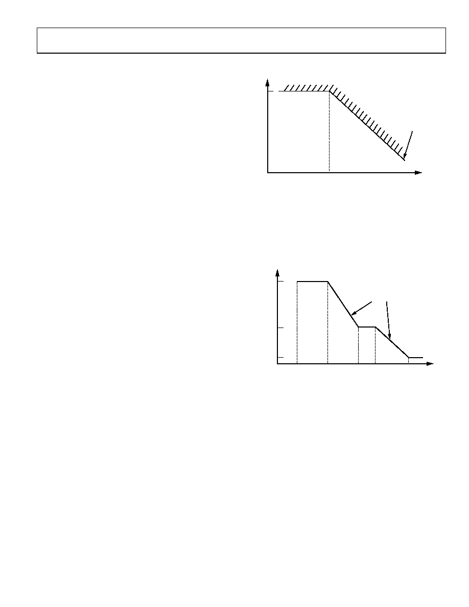
Jitter Transfer
The jitter transfer function is the ratio of the jitter on the output
signal to the jitter applied on the input signal vs. the frequency.
This parameter measures the limited amount of the jitter on an
input signal that can be transferred to the output signal (see
04948-0-015
0.1
ACCEPTABLE
RANGE
fC
JITTER FREQUENCY (kHz)
SLOPE = –20dB/DECADE
J
ITTER
GA
IN
(dB
)
Figure 11. Jitter Transfer Curve
Jitter Tolerance
The jitter tolerance is defined as the peak-to-peak amplitude of
the sinusoidal jitter applied on the input signal, which causes a
1 dB power penalty. This is a stress test intended to ensure that
no additional penalty is incurred under the operating
conditions (see Figure 12).
04948-0-016
15.00
1.50
0.15
f0
f1
f2
f3
f4
JITTER FREQUENCY (kHz)
SLOPE = –20dB/DECADE
INPUT
JITTER
AMPLITUDE
(UI
p-p)
Figure 12. SONET Jitter Tolerance Mask
相关PDF资料 |
PDF描述 |
|---|---|
| MS27473T18F35S | CONN PLUG 66POS STRAIGHT W/SCKT |
| V150B24M150B3 | CONVERTER MOD DC/DC 24V 150W |
| ATA6620-TASY | IC TXRX LIN BUS 5V/50MA 8SOIC |
| AD9523-1BCPZ | IC INTEGER-N CLCK GEN 72LFCSP |
| ATA6620-TAQY | IC TXRX LIN BUS 5V/50MA 8SOIC |
相关代理商/技术参数 |
参数描述 |
|---|---|
| ADN2816ACPZ | 制造商:Analog Devices 功能描述:CLOCK & DATA RECOVERY, 160MHZ, 111mA, LF |
| ADN2816ACPZ-500RL7 | 功能描述:IC CLK/DATA REC 675MBPS 32-LFCSP RoHS:是 类别:集成电路 (IC) >> 时钟/计时 - 专用 系列:- 标准包装:28 系列:- 类型:时钟/频率发生器 PLL:是 主要目的:Intel CPU 服务器 输入:时钟 输出:LVCMOS 电路数:1 比率 - 输入:输出:3:22 差分 - 输入:输出:无/是 频率 - 最大:400MHz 电源电压:3.135 V ~ 3.465 V 工作温度:0°C ~ 85°C 安装类型:表面贴装 封装/外壳:64-TFSOP (0.240",6.10mm 宽) 供应商设备封装:64-TSSOP 包装:管件 |
| ADN2816ACPZ-RL7 | 功能描述:IC CLK/DATA REC 675MBPS 32-LFCSP RoHS:是 类别:集成电路 (IC) >> 时钟/计时 - 专用 系列:- 标准包装:28 系列:- 类型:时钟/频率发生器 PLL:是 主要目的:Intel CPU 服务器 输入:时钟 输出:LVCMOS 电路数:1 比率 - 输入:输出:3:22 差分 - 输入:输出:无/是 频率 - 最大:400MHz 电源电压:3.135 V ~ 3.465 V 工作温度:0°C ~ 85°C 安装类型:表面贴装 封装/外壳:64-TFSOP (0.240",6.10mm 宽) 供应商设备封装:64-TSSOP 包装:管件 |
| ADN2816XCPZ | 制造商:AD 制造商全称:Analog Devices 功能描述:Continuous Rate 12.3 Mb/s to 675 Mb/s Clock and Data Recovery IC |
| ADN2817 | 制造商:AD 制造商全称:Analog Devices 功能描述:Continuous Rate 12.3Mb/s to 2.7Gb/s Clock and Data Recovery ICs |
发布紧急采购,3分钟左右您将得到回复。