- 您现在的位置:买卖IC网 > PDF目录1990 > ADN2819ACPZ-CML (Analog Devices Inc)IC CLOCK/DATA RECOVERY 48LFCSP PDF资料下载
参数资料
| 型号: | ADN2819ACPZ-CML |
| 厂商: | Analog Devices Inc |
| 文件页数: | 13/24页 |
| 文件大小: | 0K |
| 描述: | IC CLOCK/DATA RECOVERY 48LFCSP |
| 标准包装: | 1 |
| 类型: | 时钟和数据恢复(CDR),多路复用器 |
| PLL: | 是 |
| 主要目的: | SONET/SDH,STM |
| 输入: | CML |
| 输出: | CML |
| 电路数: | 1 |
| 比率 - 输入:输出: | 1:2 |
| 差分 - 输入:输出: | 是/是 |
| 频率 - 最大: | 2.7GHz |
| 电源电压: | 3 V ~ 3.6 V |
| 工作温度: | -40°C ~ 85°C |
| 安装类型: | 表面贴装 |
| 封装/外壳: | 48-VFQFN 裸露焊盘,CSP |
| 供应商设备封装: | 48-LFCSP |
| 包装: | 托盘 |
ADN2819
Rev. B | Page 20 of 24
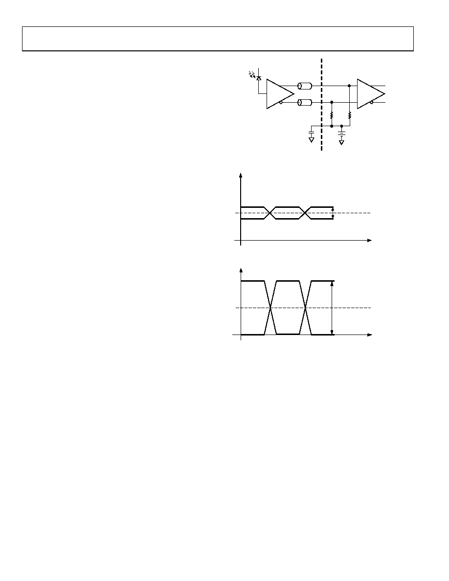
DC-COUPLED APPLICATION
The inputs to the ADN2819 can also be dc-coupled. This may
be necessary in burst mode applications where there are long
periods of CIDs and baseline wander cannot be tolerated. If the
inputs to the ADN2819 are dc-coupled, care must be taken not
to violate the input range and common-mode level
requirements of the ADN2819 (see Figure 26, Figure 27, and
Figure 28). If dc-coupling is required, and the output levels of
the TIA do not adhere to the levels shown in Figure 27 and
Figure 28, there needs to be level shifting and/or an attenuator
between the TIA outputs and the ADN2819 inputs.
LOL TOGGLING DURING LOSS OF INPUT DATA
If the input data stream is lost due to a break in the optical link
(or for any reason), the clock output from the ADN2819 will
stay within 1000 ppm of the VCO center frequency as long as
there is a valid reference clock. The LOL pin toggles at a rate of
several kHz because the LOL pin toggles between a Logic 1 and
a Logic 0, while the frequency loop and phase loop swap control
of the VCO. The chain of events is as follows:
The ADN2819 is locked to the input data stream; LOL = 0.
The input data stream is lost due to a break in the link. The
VCO frequency drifts until the frequency error is greater
than 1000 ppm. LOL is asserted to a Logic 1 as control of
the VCO is passed back to the frequency loop.
The frequency loop pulls the VCO to within 500 ppm of its
center frequency. Control of the VCO is passed back to the
phase loop and LOL is deasserted to a Logic 0.
The phase loop tries to acquire, but there is no input data
present so the VCO frequency drifts.
The VCO frequency drifts until the frequency error is
greater than 1000 ppm. LOL is asserted to a Logic 1 as
control of the VCO is passed back to the frequency loop.
This process is repeated until a valid input data stream is
re-established.
50
50
ADN2819
0.1
F
NIN
PIN
50
TIA
VREF
VCC
50
02999-B
-026
Figure 26. ADN2819 with DC-Coupled Inputs
VCM = 0.4V MIN
(DC-COUPLED)
VSE = 5mV MIN
PIN
NIN
V p-p = PIN – NIN = 2
× V
SE = 10mV AT SENSITIVITY
INPUT (V)
02999-
B-
027
Figure 27. Minimum Allowed DC-Coupled Input Levels
INPUT (V)
PIN
NIN
VCM = 0.6V
(DC-COUPLED)
VSE = 1.2V MAX
V p-p = PIN – NIN = 2
× V
SE = 2.4V MAX
02999-
B-
028
Figure 28. Maximum Allowed DC-Coupled Input Levels
相关PDF资料 |
PDF描述 |
|---|---|
| ADN2855ACPZ-R7 | IC CLK/RECOVERY MULTI 32LFCSP |
| ADS1191IPBS | IC AFE 16BIT 8KSPS 1CH 32TQFP |
| ADS1222IPWTG4 | IC 24BIT ADC W/2CH MUX 14-TSSOP |
| ADS1234IPWG4 | IC ADC 24BIT BRDG SENSOR 28TSSOP |
| ADS1241EG4 | IC ADC 24-BIT SER PROGBL 28-SSOP |
相关代理商/技术参数 |
参数描述 |
|---|---|
| ADN2819ACPZ-CML1 | 制造商:AD 制造商全称:Analog Devices 功能描述:Multirate to 2.7 Gb/s Clock and Data Recovery IC with Integrated Limiting Amp |
| ADN2819ACPZ-CML-RL | 功能描述:IC CLOCK/DATA RECOVERY 48LFCSP RoHS:是 类别:集成电路 (IC) >> 时钟/计时 - 专用 系列:- 标准包装:28 系列:- 类型:时钟/频率发生器 PLL:是 主要目的:Intel CPU 服务器 输入:时钟 输出:LVCMOS 电路数:1 比率 - 输入:输出:3:22 差分 - 输入:输出:无/是 频率 - 最大:400MHz 电源电压:3.135 V ~ 3.465 V 工作温度:0°C ~ 85°C 安装类型:表面贴装 封装/外壳:64-TFSOP (0.240",6.10mm 宽) 供应商设备封装:64-TSSOP 包装:管件 |
| ADN2819ACPZ-CML-RL1 | 制造商:AD 制造商全称:Analog Devices 功能描述:Multirate to 2.7 Gb/s Clock and Data Recovery IC with Integrated Limiting Amp |
| ADN2820 | 制造商:AD 制造商全称:Analog Devices 功能描述:10.7 Gbps, 3.3V, Low Noise, TIA with Average Power Moniter |
| ADN2820ACHIPS | 制造商:Analog Devices 功能描述: |
发布紧急采购,3分钟左右您将得到回复。