- 您现在的位置:买卖IC网 > PDF目录1990 > ADN2819ACPZ-CML (Analog Devices Inc)IC CLOCK/DATA RECOVERY 48LFCSP PDF资料下载
参数资料
| 型号: | ADN2819ACPZ-CML |
| 厂商: | Analog Devices Inc |
| 文件页数: | 5/24页 |
| 文件大小: | 0K |
| 描述: | IC CLOCK/DATA RECOVERY 48LFCSP |
| 标准包装: | 1 |
| 类型: | 时钟和数据恢复(CDR),多路复用器 |
| PLL: | 是 |
| 主要目的: | SONET/SDH,STM |
| 输入: | CML |
| 输出: | CML |
| 电路数: | 1 |
| 比率 - 输入:输出: | 1:2 |
| 差分 - 输入:输出: | 是/是 |
| 频率 - 最大: | 2.7GHz |
| 电源电压: | 3 V ~ 3.6 V |
| 工作温度: | -40°C ~ 85°C |
| 安装类型: | 表面贴装 |
| 封装/外壳: | 48-VFQFN 裸露焊盘,CSP |
| 供应商设备封装: | 48-LFCSP |
| 包装: | 托盘 |
ADN2819
Rev. B | Page 13 of 24
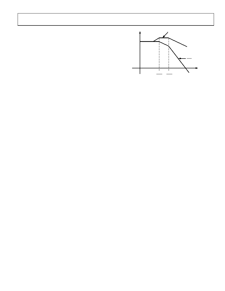
The gain of the loop integrator is small for high jitter
frequencies, so larger phase differences are needed to make the
loop control voltage big enough to tune the range of the phase
shifter. Large phase errors at high jitter frequencies cannot be
tolerated. In this region, the gain of the integrator determines
the jitter accommodation. Since the gain of the loop integrator
declines linearly with frequency, jitter accommodation is lower
with higher jitter frequency. At the highest frequencies, the loop
gain is very small and little tuning of the phase shifter can be
expected. In this case, jitter accommodation is determined by
the eye opening of the input data, the static phase error, and the
residual loop jitter generation. The jitter accommodation is
roughly 0.5 UI in this region. The corner frequency between the
declining slope and the flat region is the closed-loop bandwidth
of the delay-locked loop, which is roughly 5 MHz for OC-12,
OC-48, and GbE data rates, and 600 kHz for OC-3 data rates.
JITTER PEAKING
IN ORDINARY PLL
ADN2819
Z(s)
X(s)
f (kHz)
JITTER
GAIN
(dB)
o
n psh
d psh
c
02999-B
-016
Figure 16. Jitter Response vs. Conventional PLL
相关PDF资料 |
PDF描述 |
|---|---|
| ADN2855ACPZ-R7 | IC CLK/RECOVERY MULTI 32LFCSP |
| ADS1191IPBS | IC AFE 16BIT 8KSPS 1CH 32TQFP |
| ADS1222IPWTG4 | IC 24BIT ADC W/2CH MUX 14-TSSOP |
| ADS1234IPWG4 | IC ADC 24BIT BRDG SENSOR 28TSSOP |
| ADS1241EG4 | IC ADC 24-BIT SER PROGBL 28-SSOP |
相关代理商/技术参数 |
参数描述 |
|---|---|
| ADN2819ACPZ-CML1 | 制造商:AD 制造商全称:Analog Devices 功能描述:Multirate to 2.7 Gb/s Clock and Data Recovery IC with Integrated Limiting Amp |
| ADN2819ACPZ-CML-RL | 功能描述:IC CLOCK/DATA RECOVERY 48LFCSP RoHS:是 类别:集成电路 (IC) >> 时钟/计时 - 专用 系列:- 标准包装:28 系列:- 类型:时钟/频率发生器 PLL:是 主要目的:Intel CPU 服务器 输入:时钟 输出:LVCMOS 电路数:1 比率 - 输入:输出:3:22 差分 - 输入:输出:无/是 频率 - 最大:400MHz 电源电压:3.135 V ~ 3.465 V 工作温度:0°C ~ 85°C 安装类型:表面贴装 封装/外壳:64-TFSOP (0.240",6.10mm 宽) 供应商设备封装:64-TSSOP 包装:管件 |
| ADN2819ACPZ-CML-RL1 | 制造商:AD 制造商全称:Analog Devices 功能描述:Multirate to 2.7 Gb/s Clock and Data Recovery IC with Integrated Limiting Amp |
| ADN2820 | 制造商:AD 制造商全称:Analog Devices 功能描述:10.7 Gbps, 3.3V, Low Noise, TIA with Average Power Moniter |
| ADN2820ACHIPS | 制造商:Analog Devices 功能描述: |
发布紧急采购,3分钟左右您将得到回复。