参数资料
| 型号: | ADN2891ACPZ-RL |
| 厂商: | Analog Devices Inc |
| 文件页数: | 3/16页 |
| 文件大小: | 0K |
| 描述: | IC AMP LIM 16LFCSP |
| 标准包装: | 5,000 |
| 放大器类型: | 限制 |
| 电路数: | 1 |
| 输出类型: | 差分 |
| 电压 - 输入偏移: | 100µV |
| 电流 - 电源: | 45mA |
| 电压 - 电源,单路/双路(±): | 2.9 V ~ 3.6 V |
| 工作温度: | -40°C ~ 95°C |
| 安装类型: | 表面贴装 |
| 封装/外壳: | 16-VFQFN 裸露焊盘,CSP |
| 供应商设备封装: | 16-LFCSP-VQ |
| 包装: | 带卷 (TR) |
ADN2891
Rev. A | Page 11 of 16
APPLICATIONS
PCB DESIGN GUIDELINES
The exposed pad should connect to the GND plane using filled
vias so that solder does not leak through the vias during reflow.
Using filled vias in parallel under the package greatly reduces
the thermal resistance and enhances the reliability of the
connectivity of the exposed pad to the GND plane during
reflow.
Proper RF PCB design techniques must be used to ensure
optimal performance.
Output Buffer Power Supply and Ground Planes
Pin 9 (DRVEE) and Pin 12 (DRVCC) are the power supply and
ground pins that provide current to the differential output
buffer. To reduce possible series inductance, Pin 9, which is the
ground return of the output buffer, should connect to ground
directly. If the ground plane is an internal plane and
connections to the ground plane are vias, multiple vias in
parallel to ground can reduce series inductance.
To reduce power noise, a 10 μF electrolytic decoupling capacitor
between power and ground should be close to where the 3.3 V
supply enters the PCB. The other 0.1 μF and 1 nF ceramic chip
decoupling capacitors should be close to the VCC and VEE pins
to provide better decouple filtering and a shorter current return
loop.
Similarly, to reduce the possible series inductance, Pin 12,
which supplies power to the high speed differential
OUTP/OUTN output buffer, should connect to the power plane
directly. If the power plane is an internal plane and connections
to the power plane are vias, multiple vias in parallel can reduce
the series inductance, especially on Pin 12. See Figure 20 for the
recommended connections.
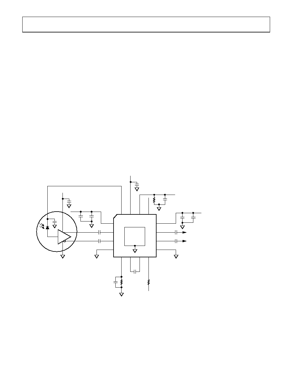
05244-
008
CONNECT
EXPOSED
PAD TO
GND
AVCC
1
THRADJ
5
CAZ1
6
CAZ2
7
LOS
8
PD_
C
ATHODE
16
PD_VCC
15
RSSI_OUT
14
SQUELCH
13
PIN
2
NIN
3
AVEE
4
DRVCC
12
OUTN
10
DRVEE
9
OUTP
C4
C3
11
C2
C1
TO HOST
BOARD
C7
C8
VCC
C5
C6
VCC
C11
C12
R2
VCC
R3
4.7k
Ω TO 10kΩ
ON HOST BOARD
VCC
ADN2880
0.1
μF
VCC
C9
RSSI MEASUREMENT
TO ADC
R1
C10
C1–C4, C11: 0.01
μF X5R/X7R DIELECTRIC, 0201 CASE
C5, C7, C9, C10, C12: 0.1
μF X5R/X7R DIELECTRIC, 0402 CASE
C6, C8: 1nF X5R/X7R DIELECTRIC, 0201 CASE
ADN2891
Figure 20. Typical Applications Circuit (Example of Using PIN PD and On-Chip RSSI Detector)
相关PDF资料 |
PDF描述 |
|---|---|
| LT6235CGN | IC OP AMP QUAD 1.15MA R-R 16SSOP |
| 170M4315 | FUSE 550A 690V 1E/86 AR UC |
| 1.5KE510A-E3/54 | TVS UNIDIR 1.5KW 510V 5% 1.5KE |
| 1.5KE480A-E3/54 | TVS UNIDIR 1.5KW 480V 5% 1.5KE |
| 4-1437514-7 | CONN SOCKET MATE DIA .64-.89MM |
相关代理商/技术参数 |
参数描述 |
|---|---|
| ADN2891ACPZ-RL7 | 功能描述:IC AMP LIM 16LFCSP RoHS:是 类别:集成电路 (IC) >> Linear - Amplifiers - Instrumentation 系列:- 标准包装:2,500 系列:- 放大器类型:通用 电路数:4 输出类型:- 转换速率:0.6 V/µs 增益带宽积:1MHz -3db带宽:- 电流 - 输入偏压:45nA 电压 - 输入偏移:2000µV 电流 - 电源:1.4mA 电流 - 输出 / 通道:40mA 电压 - 电源,单路/双路(±):3 V ~ 32 V,±1.5 V ~ 16 V 工作温度:0°C ~ 70°C 安装类型:表面贴装 封装/外壳:14-TSSOP(0.173",4.40mm 宽) 供应商设备封装:14-TSSOP 包装:带卷 (TR) 其它名称:LM324ADTBR2G-NDLM324ADTBR2GOSTR |
| ADN2891ACPZ-WP | 制造商:Analog Devices 功能描述:SP Amp Limiting Amp Single 3.6V 16-Pin LFCSP EP Tray 制造商:Analog Devices 功能描述:SP AMP LIMITING AMP SGL 3.6V 16LFCSP EP - Waffle Pack 制造商:Analog Devices 功能描述:APC12.7GBPS LIMITING AMPLIFIER.I.C. |
| ADN2891XCPZ | 制造商:Analog Devices 功能描述:- Trays |
| ADN2892 | 制造商:AD 制造商全称:Analog Devices 功能描述:3.3 V 4.25 Gb/s Limiting Amplifier |
| ADN2892ACP-RL | 制造商:AD 制造商全称:Analog Devices 功能描述:3.3 V 4.25 Gb/s Limiting Amplifier |
发布紧急采购,3分钟左右您将得到回复。