参数资料
| 型号: | ADN2891ACPZ-RL |
| 厂商: | Analog Devices Inc |
| 文件页数: | 4/16页 |
| 文件大小: | 0K |
| 描述: | IC AMP LIM 16LFCSP |
| 标准包装: | 5,000 |
| 放大器类型: | 限制 |
| 电路数: | 1 |
| 输出类型: | 差分 |
| 电压 - 输入偏移: | 100µV |
| 电流 - 电源: | 45mA |
| 电压 - 电源,单路/双路(±): | 2.9 V ~ 3.6 V |
| 工作温度: | -40°C ~ 95°C |
| 安装类型: | 表面贴装 |
| 封装/外壳: | 16-VFQFN 裸露焊盘,CSP |
| 供应商设备封装: | 16-LFCSP-VQ |
| 包装: | 带卷 (TR) |
ADN2891
Rev. A | Page 12 of 16
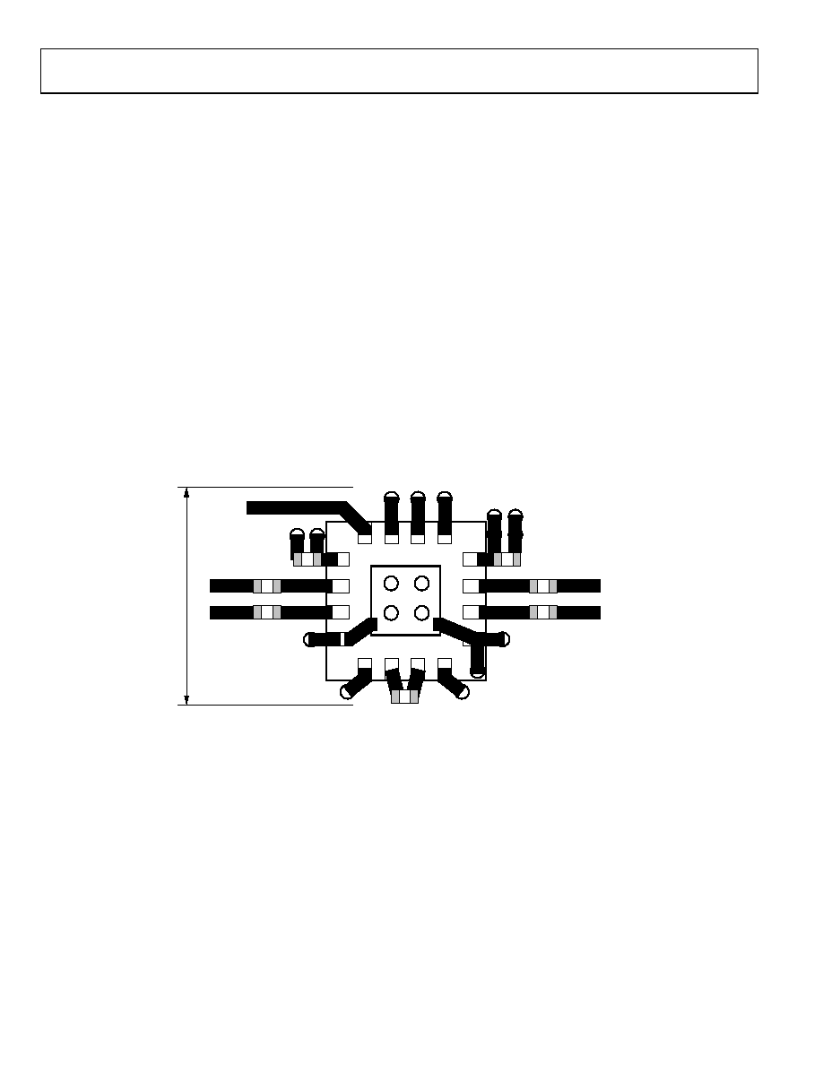
PCB Layout
As with any high speed, mixed-signal design, keep all high
speed digital traces away from sensitive analog nodes.
Figure 21 shows the recommended PCB layout. The 50 Ω
transmission lines are the traces that bring the high frequency
input and output signals (PIN, NIN, OUTP, and OUTN) to the
SMA connectors with minimum reflection. To avoid a signal
skew between the differential traces, each differential PIN/NIN
and OUTP/OUTN pair should have matched trace lengths from
the signal pins to the corresponding SMA connectors. C1, C2,
C3, and C4 are ac coupling capacitors in series with the high
speed, signal input/output paths. To minimize the possible
mismatch, the ac coupling capacitor pads should be the same
width as the 50 Ω transmission line trace width. To reduce
supply noise, a 1 nF decoupling capacitor should be placed on
the same layer as close as possible to the VCC pins. A 0.1 μF
decoupling capacitor can be placed on the bottom of the PCB
directly underneath the 1 nF capacitor. All high speed, CML
outputs have internal 50 Ω resistor termination between the
output pin and VCC. The high speed inputs, PIN and NIN, also
have the internal 50 Ω termination to an internal reference
voltage.
Soldering Guidelines for the LFCSP
The lands on the 16-lead LFCSP are rectangular. The PCB pad
for these should be 0.1 mm longer than the package land length
and 0.05 mm wider than the package land width. The land
should be centered on the pad. This ensures that the solder joint
size is maximized. The bottom of the LFCSP has a central
exposed pad. The pad on the printed circuit board should be at
least as large as the exposed pad. Users must connect the
exposed pad to VEE using filled vias so that solder does not
leak through the vias during reflow. This ensures a solid
connection from the exposed pad to VEE.
05244-009
1
VIAS TO
GND
EXPOSED PAD
PIN
NIN
VIA TO C12, R2
ON BOTTOM
C11
VIA TO BOTTOM
C3
C8
C4
C1
C6
C2
OUTP
DOUBLE-VIAS TO REDUCE
INDUCTANCE TO SUPPLY
AND GND
R1, C9, C10 ON BOTTOM
TO ROSA
PLACE C7 ON
BOTTOM OF BOARD
UNDERNEATH C8
OUTN
PLACE C5 ON
BOTTOM OF BOARD
UNDERNEATH C6
4mm
DOUBLE-VIA TO GND
TO REDUCE INDUCTANCE
Figure 21. Recommended PCB Layout (Top View)
相关PDF资料 |
PDF描述 |
|---|---|
| LT6235CGN | IC OP AMP QUAD 1.15MA R-R 16SSOP |
| 170M4315 | FUSE 550A 690V 1E/86 AR UC |
| 1.5KE510A-E3/54 | TVS UNIDIR 1.5KW 510V 5% 1.5KE |
| 1.5KE480A-E3/54 | TVS UNIDIR 1.5KW 480V 5% 1.5KE |
| 4-1437514-7 | CONN SOCKET MATE DIA .64-.89MM |
相关代理商/技术参数 |
参数描述 |
|---|---|
| ADN2891ACPZ-RL7 | 功能描述:IC AMP LIM 16LFCSP RoHS:是 类别:集成电路 (IC) >> Linear - Amplifiers - Instrumentation 系列:- 标准包装:2,500 系列:- 放大器类型:通用 电路数:4 输出类型:- 转换速率:0.6 V/µs 增益带宽积:1MHz -3db带宽:- 电流 - 输入偏压:45nA 电压 - 输入偏移:2000µV 电流 - 电源:1.4mA 电流 - 输出 / 通道:40mA 电压 - 电源,单路/双路(±):3 V ~ 32 V,±1.5 V ~ 16 V 工作温度:0°C ~ 70°C 安装类型:表面贴装 封装/外壳:14-TSSOP(0.173",4.40mm 宽) 供应商设备封装:14-TSSOP 包装:带卷 (TR) 其它名称:LM324ADTBR2G-NDLM324ADTBR2GOSTR |
| ADN2891ACPZ-WP | 制造商:Analog Devices 功能描述:SP Amp Limiting Amp Single 3.6V 16-Pin LFCSP EP Tray 制造商:Analog Devices 功能描述:SP AMP LIMITING AMP SGL 3.6V 16LFCSP EP - Waffle Pack 制造商:Analog Devices 功能描述:APC12.7GBPS LIMITING AMPLIFIER.I.C. |
| ADN2891XCPZ | 制造商:Analog Devices 功能描述:- Trays |
| ADN2892 | 制造商:AD 制造商全称:Analog Devices 功能描述:3.3 V 4.25 Gb/s Limiting Amplifier |
| ADN2892ACP-RL | 制造商:AD 制造商全称:Analog Devices 功能描述:3.3 V 4.25 Gb/s Limiting Amplifier |
发布紧急采购,3分钟左右您将得到回复。