- 您现在的位置:买卖IC网 > PDF目录11354 > ADN4604ASVZ (Analog Devices Inc)IC CROSSPOINT SWIT 16X16 100TQFP PDF资料下载
参数资料
| 型号: | ADN4604ASVZ |
| 厂商: | Analog Devices Inc |
| 文件页数: | 11/40页 |
| 文件大小: | 0K |
| 描述: | IC CROSSPOINT SWIT 16X16 100TQFP |
| 标准包装: | 1 |
| 系列: | XStream™ |
| 功能: | 交叉点开关 |
| 电路: | 1 x 16:16 |
| 电压电源: | 单电源 |
| 电压 - 电源,单路/双路(±): | 2.7 V ~ 3.6 V |
| 电流 - 电源: | 95mA |
| 工作温度: | -40°C ~ 85°C |
| 安装类型: | 表面贴装 |
| 封装/外壳: | 100-TQFP 裸露焊盘 |
| 供应商设备封装: | 100-TQFP-EP(14x14) |
| 包装: | 托盘 |
第1页第2页第3页第4页第5页第6页第7页第8页第9页第10页当前第11页第12页第13页第14页第15页第16页第17页第18页第19页第20页第21页第22页第23页第24页第25页第26页第27页第28页第29页第30页第31页第32页第33页第34页第35页第36页第37页第38页第39页第40页
Data Sheet
ADN4604
Rev. A | Page 19 of 40
TRANSMITTERS
The ADN4604 transmitter outputs incorporate 50 Ω termin-
ation resistors, ESD protection, and output current switches.
Each channel provides independent control of both the absolute
output level and the preemphasis output level. Note that the
choice of output level affects the output common-mode level.
ON-CHIP TERMINATION
ESD
VCC
VTTOx
OPx
ONx
VEE
V3
VC
V2
VP
V1
VN
Q1
IT
IDC + IPE
Q2
RP
50
RN
50
079
34-
04
2
Figure 42. Simplified TX Output Circuit
Preemphasis
Transmission line attenuation can be equalized at the trans-
mitter using preemphasis. The transmit equalizer setting can
be chosen by matching the channel loss to the amount of boost
provided by the preemphasis.
Basic Settings
In the basic mode of operation, predefined preemphasis settings
are available through a lookup table. Each table entry requires
two bytes of memory. The amount of preemphasis provided
is independent of the full-scale current output. Transmitter
preemphasis levels, as well as dc output levels, can be set
through the serial control interface. The output level and
amount of preemphasis can be independently programmed
through advanced registers. By default, however, the total
output amplitude and preemphasis setting space is reduced
to a single table of basic settings that provides eight levels of
output equalization to ease programming for typical FR4
channels.
Table 10 summarizes the absolute output level, preemphasis
level, and high frequency boost for control setting. The full
resolution of eight settings is available through the serial
interface by writing to Bits[2:0] (the TX PE[2:0] bits) of the
Basic TX Control registers shown in Table 11. A single setting
is programmed to all outputs simultaneously by writing to the
0x18 broadcast address.
The TX has four possible output enable states (disabled,
standby, squelched, and enabled) controlled by the TX EN[1:0]
bits as shown in Table 11. Disabled is the lowest power-down
state. When squelched, the output voltage at both P and N
outputs will be the common-mode voltage as defined by the
output current settings. In standby, the output level of both P
and N outputs will be pulled up to the termination supply
(VTTON or VTTOS).
The TX CTL SELECT bit (Bit 6) in the TX[15:0] basic control
register determines whether the preemphasis and output
current controls for the channel of interest are selected from
the predefined lookup table or directly from the TX[15:0]
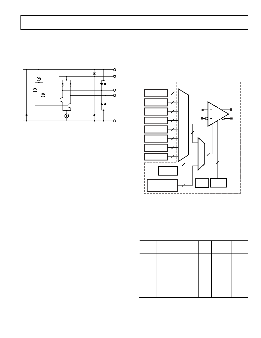
Drive Control[1:0] registers (per channel). Figure 43 is an
illustration of the TX control circuit. Setting the TX CTL
SELECT bit low (default setting) selects preemphasis control
from the predefined, optimized lookup table (Address 0x60
to Address 0x6F).
07
93
4-
04
3
TABLE
ENTRY 0
TABLE
ENTRY 1
TABLE
ENTRY 2
TABLE
ENTRY 3
TABLE
ENTRY 4
TABLE
ENTRY 5
TABLE
ENTRY 6
TABLE
ENTRY 7
16
3
PE[2:0]
TX CTL
SELECT
IPx
OPx
INx
ONx
TX
PER OUTPUT PORT
LOOKUP TABLE
BASIC SETTINGS
PER PORT
OUTPUT LEVEL
ADVANCED SETTINGS
TX EN[1:0]
2
Figure 43. Transmitter Control Block Diagram
In applications where the default preemphasis settings in the
lookup table are not sufficient, the lookup table entries can be
modified by programming the TX lookup table registers (0x60
to 0x6F) shown in Table 12. In applications where the eight
table entries are insufficient, each output can be programmed
individually.
Table 10. Preemphasis Boost and Overshoot vs. Setting
PE
Setting
Main Tap
Current
(mA)
Delayed Tap
Current (mA)
Boost
(dB)
Overshoot
(%)
DC Swing
(mV p-p)
0
16
0
0.0
0
800
1
16
2
2.0
25
800
2
16
5
4.2
62.5
800
3
16
8
6.0
100
800
4
11
8
7.8
145
550
5
8
9.5
200
400
6
4
6
12.0
300
7
4
6
12.0
300
相关PDF资料 |
PDF描述 |
|---|---|
| GRM319R71E394KA01D | CAP CER 0.39UF 25V 10% X7R 1206 |
| ADV3229ACPZ | IC CROSSPOINT SW 16X8 72LFCSP |
| PIC24HJ64GP210AT-I/PF | IC PIC MCU FLASH 64KB 100-TQFP |
| PIC16C57-LPE/SO | IC MCU OTP 2KX12 28SOIC |
| PIC24HJ128GP306A-E/MR | IC PIC MCU FLASH 128KB 64-QFN |
相关代理商/技术参数 |
参数描述 |
|---|---|
| ADN4604ASVZ-RL | 功能描述:IC CROSSPOINT SWIT 16X16 100TQFP RoHS:是 类别:集成电路 (IC) >> 接口 - 模拟开关,多路复用器,多路分解器 系列:XStream™ 其它有关文件:STG4159 View All Specifications 标准包装:5,000 系列:- 功能:开关 电路:1 x SPDT 导通状态电阻:300 毫欧 电压电源:双电源 电压 - 电源,单路/双路(±):±1.65 V ~ 4.8 V 电流 - 电源:50nA 工作温度:-40°C ~ 85°C 安装类型:表面贴装 封装/外壳:7-WFBGA,FCBGA 供应商设备封装:7-覆晶 包装:带卷 (TR) |
| ADN4604-EVALZ | 制造商:Analog Devices 功能描述:EVALUATION BOARD - Boxed Product (Development Kits) |
| ADN4604XSVZ | 制造商:Analog Devices 功能描述:4.25GBPS 16X16 CROSSBAR SWITCH - Trays |
| ADN4605 | 制造商:AD 制造商全称:Analog Devices 功能描述:4.25 Gbps 40 × 40 Digital Crosspoint Switch 3 dB, 6 dB, or 12 dB boost |
| ADN4605_1111 | 制造商:AD 制造商全称:Analog Devices 功能描述:4.25 Gbps 40 ?? 40 Digital |
发布紧急采购,3分钟左右您将得到回复。