- 您现在的位置:买卖IC网 > PDF目录16944 > ADP122-3.3-EVALZ (Analog Devices Inc)BOARD EVALUATION 3.3V ADP122 PDF资料下载
参数资料
| 型号: | ADP122-3.3-EVALZ |
| 厂商: | Analog Devices Inc |
| 文件页数: | 12/24页 |
| 文件大小: | 0K |
| 描述: | BOARD EVALUATION 3.3V ADP122 |
| 标准包装: | 1 |
| 每 IC 通道数: | 1 - 单 |
| 输出电压: | 3.3V |
| 电流 - 输出: | 300mA |
| 输入电压: | 2.3 ~ 5.5 V |
| 稳压器类型: | 正,固定式 |
| 工作温度: | -40°C ~ 85°C |
| 板类型: | 完全填充 |
| 已供物品: | 板 |
| 已用 IC / 零件: | ADP122 |
�� ��
��
��ADP122/ADP123�
�APPLICATIONS� INFORMATION�
�CAPACITOR� SELECTION�
�Output� Capacitor�
�The� ADP122/ADP123� are� designed� for� operation� with� small,�
�space-saving� ceramic� capacitors,� but� these� devices� can� function�
�with� most� commonly� used� capacitors� as� long� as� care� is� taken� to�
�ensure� an� appropriate� effective� series� resistance� (ESR)� value.� The�
�ESR� of� the� output� capacitor� affects� the� stability� of� the� LDO� control�
�loop.� A� minimum� of� 0.70� μF� capacitance� with� an� ESR� of� 1� ?� or�
�less� is� recommended� to� ensure� stability� of� the� ADP122/ADP123.�
�The� transient� response� to� changes� in� load� current� is� also� affected� by�
�the� output� capacitance.� Using� a� larger� value� of� output� capacitance�
�improves� the� transient� response� of� the� ADP122/ADP123� to�
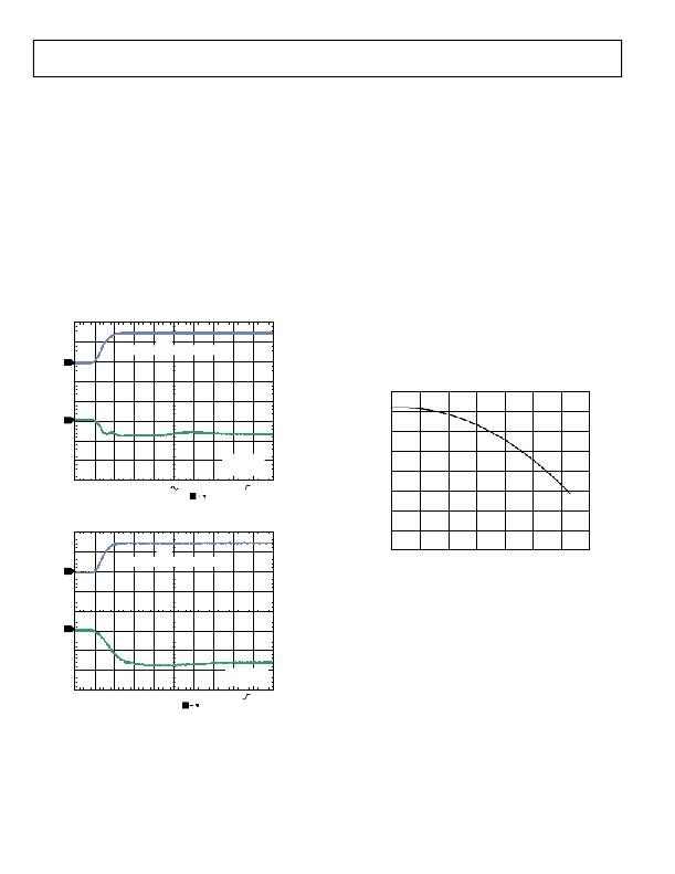
�dynamic� changes� in� load� current.� Figure� 32� and� Figure� 33� show�
�the� transient� responses� for� output� capacitance� values� of� 1� μF� and�
�4.7� μF,� respectively.�
�I� OUT�
�1mA� TO� 300mA� LOAD� STEP�
�1�
�Data� Sheet�
�Input� and� Output� Capacitor� Properties�
�Any� good� quality� ceramic� capacitors� can� be� used� with� the� ADP122/�
�ADP123,� as� long� as� the� capacitor� meets� the� minimum� capacitance�
�and� maximum� ESR� requirements.� Ceramic� capacitors� are� manu-�
�factured� with� a� variety� of� dielectrics,� each� with� different� behavior�
�over� temperature� and� applied� voltage.� Capacitors� must� have� an�
�adequate� dielectric� to� ensure� the� minimum� capacitance� over� the�
�necessary� temperature� range� and� dc� bias� conditions.� Using� an�
�X5R� or� X7R� dielectric� with� a� voltage� rating� of� 6.3� V� or� 10� V� is�
�recommended.� However,� using� Y5V� and� Z5U� dielectrics� is� not�
�recommended� for� any� LDO,� due� to� their� poor� temperature� and�
�dc� bias� characteristics.�
��teristics� of� a� 0603,� 1� μF,� 6.3� V� X5R� capacitor.� The� voltage� stability� of�
�a� capacitor� is� strongly� influenced� by� the� capacitor� size� and� the�
�voltage� rating.� In� general,� a� capacitor� in� a� larger� package� or� of� a�
�higher� voltage� rating� exhibits� better� stability.� The� temperature�
�variation� of� the� X5R� dielectric� is� about� ±15%� over� the� ?40°C� to�
�+85°C� temperature� range� and� is� not� a� function� of� package� or�
�voltage� rating.�
�1.10�
�1.05�
�2�
�V� OUT�
�V� IN� =� 3.7V�
�1.00�
�0.95�
�V� OUT� =� 3.3V�
�0.90�
�CH1� 200mA�
�?� B�
�W�
�CH2� 50.0mV�
�B�
�W�
�M� 400ns� A� CH1�
�196mA�
�0.85�
�T�
�14.80%�
�Figure� 32.� Output� Transient� Response,� C� OUT� =� 1� μF�
�I� OUT�
�0.80�
�0.75�
�0.70�
�1mA� TO� 300mA� LOAD� STEP�
�0�
�1�
�2�
�3�
�4�
�5�
�6�
�7�
�1�
�2�
�BIAS� VOLTAGE� (V)�
�Figure� 34.� Capacitance� vs.� Capacitor� Voltage� Bias� Characteristics�
�Equation� 1� can� be� used� to� determine� the� worst-case� capacitance,�
�accounting� for� capacitor� variation� over� temperature,� component�
�tolerance,� and� voltage.�
�C� EFF� =� C� � (1� ?� TEMPCO� )� � (1� ?� TOL� )�
�(1)�
�V� OUT�
�where:�
�CH1� 200mA� ?�
�B�
�W�
�CH2� 20.0mV�
�M� 400ns� A� CH1� 196mA�
�T� 15.00%�
�V� IN� =� 3.7V�
�V� OUT� =� 3.3V�
�C� EFF� is� the� effective� capacitance� at� the� operating� voltage.�
�TEMPCO� is� the� worst-case� capacitor� temperature� coefficient.�
�TOL� is� the� worst-case� component� tolerance.�
�Figure� 33.� Output� Transient� Response,� C� OUT� =� 4.7� μF�
�Input� Bypass� Capacitor�
�Connecting� a� 1� μF� capacitor� from� VIN� to� GND� reduces� the� circuit�
�sensitivity� to� the� printed� circuit� board� (PCB)� layout,� especially�
�when� a� long� input� trace� or� high� source� impedance� is� encountered.�
�If� greater� than� 1� μF� of� output� capacitance� is� required,� the� input�
�capacitor� should� be� increased� to� match� it.�
�In� this� example,� the� worst-case� temperature� coefficient� (TEMPCO)�
�over� ?40°C� to� +85°C� is� assumed� to� be� 15%� for� an� X5R� dielectric.�
�The� tolerance� of� the� capacitor� (TOL)� is� assumed� to� be� 10%,� and�
��Substituting� these� values� in� Equation� 1� yields�
�C� EFF� =� 0.96� μF� ×� (1� ?� 0.15)� ×� (1� ?� 0.1)� =� 0.734� μF�
�Rev.� E� |� Page� 12� of� 24�
�相关PDF资料 |
PDF描述 |
|---|---|
| VE-JVR-EY | CONVERTER MOD DC/DC 7.5V 50W |
| VE-JVP-EY | CONVERTER MOD DC/DC 13.8V 50W |
| 879364-000 | BOOT MOLDED |
| LGU2E681MELA | CAP ALUM 680UF 250V 20% SNAP |
| VE-JVX-EY | CONVERTER MOD DC/DC 5.2V 50W |
相关代理商/技术参数 |
参数描述 |
|---|---|
| ADP122ACPZ-1.8-R7 | 功能描述:IC REG LDO 1.8V .3A 6LFCSP RoHS:是 类别:集成电路 (IC) >> PMIC - 稳压器 - 线性 系列:- 其它有关文件:LD39015JXX12 View All Specifications 标准包装:1 系列:- 稳压器拓扑结构:正,固定式 输出电压:1.2V 输入电压:1.5 V ~ 5.5 V 电压 - 压降(标准):- 稳压器数量:1 电流 - 输出:150mA 电流 - 限制(最小):- 工作温度:-40°C ~ 125°C 安装类型:表面贴装 封装/外壳:4-WFBGA,FCBGA 供应商设备封装:4-覆晶(1.07x1.07) 包装:Digi-Reel® 其它名称:497-11958-6 |
| ADP122ACPZ-2.0-R7 | 功能描述:IC REG LDO 2V .3A 6LFCSP RoHS:是 类别:集成电路 (IC) >> PMIC - 稳压器 - 线性 系列:- 其它有关文件:LD39015JXX12 View All Specifications 标准包装:1 系列:- 稳压器拓扑结构:正,固定式 输出电压:1.2V 输入电压:1.5 V ~ 5.5 V 电压 - 压降(标准):- 稳压器数量:1 电流 - 输出:150mA 电流 - 限制(最小):- 工作温度:-40°C ~ 125°C 安装类型:表面贴装 封装/外壳:4-WFBGA,FCBGA 供应商设备封装:4-覆晶(1.07x1.07) 包装:Digi-Reel® 其它名称:497-11958-6 |
| ADP122ACPZ-2.5-R7 | 功能描述:IC REG LDO 2.5V .3A 6LFCSP RoHS:是 类别:集成电路 (IC) >> PMIC - 稳压器 - 线性 系列:- 其它有关文件:LD39015JXX12 View All Specifications 标准包装:1 系列:- 稳压器拓扑结构:正,固定式 输出电压:1.2V 输入电压:1.5 V ~ 5.5 V 电压 - 压降(标准):- 稳压器数量:1 电流 - 输出:150mA 电流 - 限制(最小):- 工作温度:-40°C ~ 125°C 安装类型:表面贴装 封装/外壳:4-WFBGA,FCBGA 供应商设备封装:4-覆晶(1.07x1.07) 包装:Digi-Reel® 其它名称:497-11958-6 |
| ADP122ACPZ-2.6-R7 | 功能描述:IC REG LDO 2.6V .3A 6LFCSP RoHS:是 类别:集成电路 (IC) >> PMIC - 稳压器 - 线性 系列:- 其它有关文件:LD39015JXX12 View All Specifications 标准包装:1 系列:- 稳压器拓扑结构:正,固定式 输出电压:1.2V 输入电压:1.5 V ~ 5.5 V 电压 - 压降(标准):- 稳压器数量:1 电流 - 输出:150mA 电流 - 限制(最小):- 工作温度:-40°C ~ 125°C 安装类型:表面贴装 封装/外壳:4-WFBGA,FCBGA 供应商设备封装:4-覆晶(1.07x1.07) 包装:Digi-Reel® 其它名称:497-11958-6 |
| ADP122ACPZ-2.8-R7 | 功能描述:IC REG LDO 2.8V .3A 6LFCSP RoHS:是 类别:集成电路 (IC) >> PMIC - 稳压器 - 线性 系列:- 其它有关文件:LD39015JXX12 View All Specifications 标准包装:1 系列:- 稳压器拓扑结构:正,固定式 输出电压:1.2V 输入电压:1.5 V ~ 5.5 V 电压 - 压降(标准):- 稳压器数量:1 电流 - 输出:150mA 电流 - 限制(最小):- 工作温度:-40°C ~ 125°C 安装类型:表面贴装 封装/外壳:4-WFBGA,FCBGA 供应商设备封装:4-覆晶(1.07x1.07) 包装:Digi-Reel® 其它名称:497-11958-6 |
发布紧急采购,3分钟左右您将得到回复。