- 您现在的位置:买卖IC网 > PDF目录13113 > ADP1714AUJZ-3.0-R7 (Analog Devices Inc)IC REG LDO 3V .3A 5TSOT PDF资料下载
参数资料
| 型号: | ADP1714AUJZ-3.0-R7 |
| 厂商: | Analog Devices Inc |
| 文件页数: | 11/16页 |
| 文件大小: | 0K |
| 描述: | IC REG LDO 3V .3A 5TSOT |
| 产品培训模块: | Power Line Monitoring |
| 标准包装: | 1 |
| 稳压器拓扑结构: | 正,固定式 |
| 输出电压: | 3V |
| 输入电压: | 最高 5.5V |
| 电压 - 压降(标准): | 0.17V @ 300mA |
| 稳压器数量: | 1 |
| 电流 - 输出: | 300mA(最小值) |
| 电流 - 限制(最小): | 380mA |
| 工作温度: | -40°C ~ 125°C |
| 安装类型: | 表面贴装 |
| 封装/外壳: | SOT-23-5 细型,TSOT-23-5 |
| 供应商设备封装: | TSOT-23-5 |
| 包装: | 标准包装 |
| 产品目录页面: | 794 (CN2011-ZH PDF) |
| 其它名称: | ADP1714AUJZ-3.0-R7DKR |
�� �
�
�ADP1712/ADP1713/ADP1714�
�ADJUSTABLE� OUTPUT� VOLTAGE�
�(ADP1712� ADJUSTABLE)�
�The� ADP1712� adjustable� version� can� have� its� output� voltage�
�set� over� a� 0.8� V� to� 5.0� V� range.� The� output� voltage� is� set� by�
�connecting� a� resistive� voltage� divider� from� OUT� to� ADJ.� The�
�output� voltage� is� calculated� using� the� equation�
�ENABLE� FEATURE�
�The� ADP1712/ADP1713/ADP1714� use� the� EN� pin� to� enable�
�and� disable� the� OUT� pin� under� normal� operating� conditions.�
�As� shown� in� Figure� 29,� when� a� rising� voltage� on� EN� crosses� the�
�active� threshold,� OUT� turns� on.� When� a� falling� voltage� on� EN�
�crosses� the� inactive� threshold,� OUT� turns� off.�
�V� OUT� =� 0.8� V� (1� +� R1� /� R2� )�
�where:�
�R1� is� the� resistor� from� OUT� to� ADJ.�
�R2� is� the� resistor� from� ADJ� to� GND.�
�The� maximum� bias� current� into� ADJ� is� 100� nA,� so� for� less�
�(2)�
�EN�
�than� 0.5%� error� due� to� the� bias� current,� use� values� less� than�
�60� k� for� R2.�
�BYPASS� CAPACITOR� (ADP1713)�
�The� ADP1713� allows� for� an� external� bypass� capacitor� to� be�
�connected� to� the� internal� reference,� which� reduces� output�
�voltage� noise� and� improves� power� supply� rejection.� A� low�
�leakage� capacitor� of� 1� nF� or� greater� (10� nF� is� recommended)�
�must� be� connected� between� the� BYP� and� GND� pins.�
�TRACK� MODE� (ADP1714)�
�The� ADP1714� includes� a� tracking� mode� feature.� As� shown� in�
��nominal� output� voltage,� OUT� is� equal� to� the� voltage� at� TRK.�
�Otherwise,� OUT� regulates� to� its� nominal� output� value.�
�For� example,� consider� an� ADP1714� with� a� nominal� output�
�voltage� of� 3� V.� If� the� voltage� applied� to� its� TRK� pin� is� greater� than�
�3� V,� OUT� maintains� a� nominal� output� voltage� of� 3� V.� If� the� volt-�
�age� applied� to� TRK� is� reduced� below� 3� V,� OUT� tracks� this� voltage.�
�OUT� can� track� the� TRK� pin� voltage� from� the� nominal� value� all�
�OUT�
�1�
�V� IN� =� 5V�
�V� OUT� =� 1.6V�
�C� OUT� =� 2.2� μ� F�
�I� LOAD� =� 10mA�
�TIME� (4ms/DIV)�
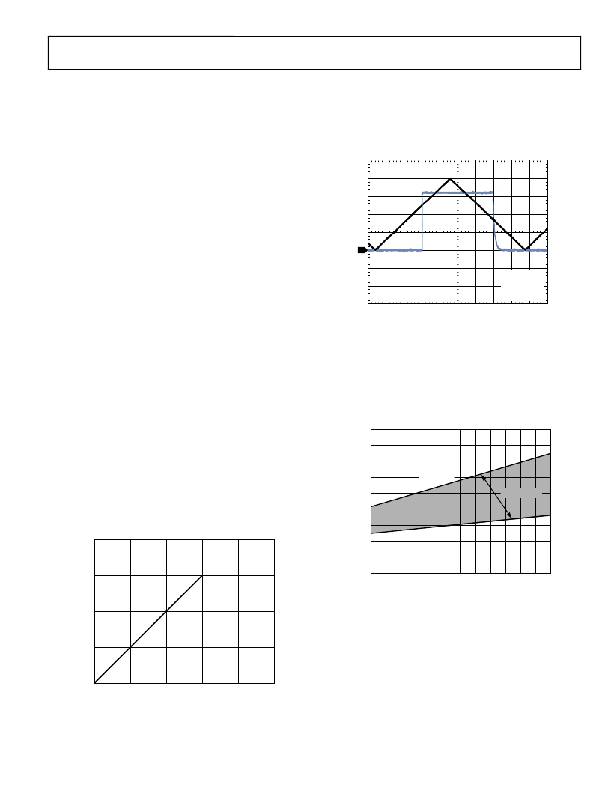
�Figure� 29.� ADP1712� Adjustable� Typical� EN� Pin� Operation�
�As� can� be� seen,� the� EN� pin� has� hysteresis� built� in.� This� prevents�
�on/off� oscillations� that� can� occur� due� to� noise� on� the� EN� pin� as�
�it� passes� through� the� threshold� points.�
�The� EN� pin� active/inactive� thresholds� are� derived� from� the� IN�
�voltage.� Therefore,� these� thresholds� vary� with� changing� input�
�voltage.� Figure� 30� shows� typical� EN� active/inactive� thresholds�
�when� the� input� voltage� varies� from� 2.5� V� to� 5.5� V.�
�1.4�
�1.3�
�1.2�
�the� way� down� to� 0� V.� A� voltage� divider� is� present� from� TRK� to� the�
�error� amplifier� input� with� a� divider� ratio� equal� to� the� divider�
�from� OUT� to� the� error� amplifier.� This� sets� the� output� voltage�
�equal� to� the� tracking� voltage.� Both� divider� ratios� are� set� by� post-�
�package� trim,� depending� on� the� desired� output� voltage.�
�4�
�1.1�
�1.0�
�0.9�
�0.8�
�0.7�
�0.6�
�EN ACTIVE�
�EN INACTIVE�
�HYSTERESIS�
�3�
�0.5�
�2.50� 2.75� 3.00� 3.25� 3.50� 3.75� 4.00� 4.25� 4.50� 4.75� 5.00� 5.25� 5.50�
�V� IN� (V)�
�Figure� 30.� Typical� EN� Pin� Thresholds� vs.� Input� Voltage�
�2�
�UNDERVOLTAGE� LOCKOUT� (UVLO)�
�The� ADP1712/ADP1713/ADP1714� have� an� undervoltage�
�1�
�lockout� circuit,� which� monitors� the� voltage� on� the� IN� pin.�
�When� the� voltage� on� IN� drops� below� 2� V� (minimum),� the�
�circuit� activates,� disabling� the� OUT� pin.�
�0�
�0�
�1�
�2�
�3�
�4�
�5�
�V� TRK� (V)�
�Figure� 28.� ADP1714� Output� Voltage� vs.� Tracking� Voltage�
�with� Nominal� Output� Voltage� Set� to� 3� V�
�Rev.� A� |� Page� 11� of� 16�
�相关PDF资料 |
PDF描述 |
|---|---|
| 400VXG120MEFCSN25X25 | CAP ALUM 120UF 400V 20% SNAP-IN |
| VE-BWL-EV-B1 | CONVERTER MOD DC/DC 28V 150W |
| EB81-S0E1260X | CONN EDGEBOARD DUAL 24POS 5A |
| 420MXH120MEFCSN22X30 | CAP ALUM 120UF 420V 20% SNAP-IN |
| GSM28DSXH | CONN EDGECARD 56POS DIP .156 SLD |
相关代理商/技术参数 |
参数描述 |
|---|---|
| ADP1714-BL1-EVZ | 制造商:Analog Devices 功能描述:Evaluation Board For Low Quiescent Current, CMOS Linear Regulators 制造商:Analog Devices 功能描述:BLANK ADISIMPOWER EVAL ADP1714 - Boxed Product (Development Kits) |
| ADP1715 | 制造商:AD 制造商全称:Analog Devices 功能描述:500 mA, Low Dropout, CMOS Linear Regulator |
| ADP1715-1.8-EVALZ | 功能描述:BOARD EVAL FOR ADP1715-1.8 RoHS:是 类别:编程器,开发系统 >> 评估板 - 线性稳压器 (LDO) 系列:- 产品变化通告:1Q2012 Discontinuation 30/Mar/2012 设计资源:NCP590MNDPTAGEVB Gerber Files 标准包装:1 系列:- 每 IC 通道数:2 - 双 输出电压:1.8V,2.8V 电流 - 输出:300mA 输入电压:2.1 ~ 5.5 V 稳压器类型:正,固定式 工作温度:-40°C ~ 85°C 板类型:完全填充 已供物品:板 已用 IC / 零件:NCP590MNDP 其它名称:NCP590MNDPTAGEVB-NDNCP590MNDPTAGEVBOS |
| ADP1715-3.3-EVALZ | 功能描述:BOARD EVAL FOR ADP1715-3.3 RoHS:是 类别:编程器,开发系统 >> 评估板 - 线性稳压器 (LDO) 系列:- 产品变化通告:1Q2012 Discontinuation 30/Mar/2012 设计资源:NCP590MNDPTAGEVB Gerber Files 标准包装:1 系列:- 每 IC 通道数:2 - 双 输出电压:1.8V,2.8V 电流 - 输出:300mA 输入电压:2.1 ~ 5.5 V 稳压器类型:正,固定式 工作温度:-40°C ~ 85°C 板类型:完全填充 已供物品:板 已用 IC / 零件:NCP590MNDP 其它名称:NCP590MNDPTAGEVB-NDNCP590MNDPTAGEVBOS |
| ADP1715ARMZ | 制造商:Analog Devices 功能描述:IC V REG LDO 0.5A ADJ SMD MSOP8 制造商:Analog Devices 功能描述:IC, V REG, LDO 0.5A ADJ, SMD, MSOP8 |
发布紧急采购,3分钟左右您将得到回复。