- 您现在的位置:买卖IC网 > PDF目录1776 > ADP1864AUJZ-R7 (Analog Devices Inc)IC REG CTRLR BUCK PWM TSOT23-6 PDF资料下载
参数资料
| 型号: | ADP1864AUJZ-R7 |
| 厂商: | Analog Devices Inc |
| 文件页数: | 12/16页 |
| 文件大小: | 0K |
| 描述: | IC REG CTRLR BUCK PWM TSOT23-6 |
| 产品培训模块: | Power Line Monitoring |
| 标准包装: | 1 |
| PWM 型: | 电流模式 |
| 输出数: | 1 |
| 频率 - 最大: | 650kHz |
| 占空比: | 100% |
| 电源电压: | 3.15 V ~ 14 V |
| 降压: | 是 |
| 升压: | 无 |
| 回扫: | 无 |
| 反相: | 无 |
| 倍增器: | 无 |
| 除法器: | 无 |
| Cuk: | 无 |
| 隔离: | 无 |
| 工作温度: | -40°C ~ 125°C |
| 封装/外壳: | SOT-23-6 细型,TSOT-23-6 |
| 包装: | 标准包装 |
| 产品目录页面: | 791 (CN2011-ZH PDF) |
| 配用: | ADP1864-EVALZ-ND - BOARD EVALUATION ADP1864 |
| 其它名称: | ADP1864AUJZ-R7DKR |
�� ��
��
��ADP1864�
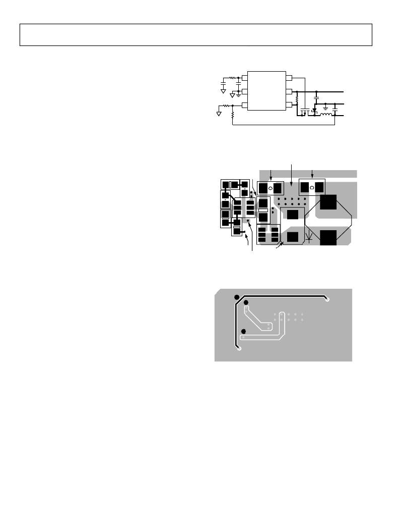
�LAYOUT� CONSIDERATIONS�
�Data� Sheet�
�Layout� is� important� with� all� switching� regulators,� but� is� particu-�
�larly� important� for� high� switching� frequencies.� Ensure� all� high�
�R2�
�1�
�COMP�
�PGATE� 6�
�current� paths� are� as� wide� as� possible� to� minimize� track� induc-�
�tance,� which� causes� spiking� and� electromagnetic� interference�
�(EMI).� These� paths� are� shown� in� bold� in� Figure� 15.� Place� the�
�current� sense� resistor� and� the� input� capacitor(s)� as� close� to� the�
�IN� pin� as� possible.�
�C2�
�C1�
�R� TOP�
�ADP1864�
�2� GND�
�3� FB�
�R� BOTTOM�
�IN� 5�
�R� S�
�CS� 4�
�U1�
�D1�
�CE1�
�L1�
�V� IN�
�PGND�
�CE2�
�V� OUT�
�Keep� the� PGND� connections� for� the� diode,� input� capacitor(s),�
�and� output� capacitor(s)� as� close� together� as� possible� on� a� wide�
�Figure� 15.� Application� Circuit� Showing� High� Current� Paths� (in� Bold)�
�PGND� plane.� Connect� the� PGND� and� GND� planes� at� a� single�
�point� with� a� narrow� trace� close� to� the� ADP1864� GND� connection.�
�Ensure� the� feedback� resistors� are� placed� as� close� as� possible�
�to� the� FB� pin� to� prevent� stray� pickup.� To� prevent� extra� noise�
�pickup� on� the� FB� line,� do� not� allow� the� feedback� trace� from�
�the� output� voltage� to� FB� to� pass� right� beside� the� drain� of� the�
�external� PFET.� Add� an� extra� copper� plane� at� the� connection� of�
�the� FET� drain� and� the� cathode� of� the� diode� to� help� dissipate� the�
�heat� generated� by� losses� in� those� components.�
�C2�
�R2�
�ISOLATED� POWER� GROUND� PLANE.� USE� A� SUBSTANTIAL�
�AMOUNT� OF� COPPER� TO� BEST� ACCOMMODATE�
�THIS� HIGH� CURRENT� PATH.� ALSO� PROVIDES� AID�
�FOR� POWER� DISSIPATION.�
�CE1� CE2�
�C1� R� S�
�V� OUT�
�All� analog� components� are� grouped� together� on� the� left� side�
�of� the� evaluation� board� (left� side� of� the� ADP1864� DUT,� see�
�R� BOTTOM�
�D1�
�L1�
��power� components� are� located� on� the� right� side� of� the� board�
�(MOSFET,� inductor,� input� bypass� capacitors,� output� capacitors,�
�and� power� diode).�
�R� TOP�
�FB� TAP�
�ANALOG�
�GROUND� TAP�
�U1�
�NOISY� POWER� PLANE� IS� LOCATED� ON� THIS�
�SIDE� OF� THE� BOARD� TO� ACCOMODATE� SPIKY�
�NODES� AND� MINIMIZE� EMI� EFFECTS� TO� THE�
�REST� OF� THE� SYSTEM.�
�All� noisy� nodes� (P-channel� drain,� power� diode� cathode,� and�
�inductor� terminal)� are� located� along� the� bottom� portion� of� the�
�evaluation� board� on� the� top� layer� (see� Figure� 16).� A� substantial�
�Figure� 16.� Top� Layer� of� an� Example� Layout� for� an� ADP1864� Application�
�amount� of� copper� has� been� allocated� for� this� area� with� ample�
�track� spacing� to� minimize� coupling� (crosstalk)� effects� during�
�switching.�
�The� FB� tap� is� isolated� and� runs� from� the� R� TOP� ,� along� the� upper�
��to� minimize� EMI� pickups� emitted� from� the� power� components�
�along� the� bottom� portion� of� the� evaluation� board’s� top� layer� (see�
��1�
�3�
�2�
�power� ground� plane� located� near� the� center� of� the� board� to�
�effectively� decouple� this� track.�
�There� are� two� ground� planes� on� the� top� layer:� the� analog�
�ground� plane� is� on� the� left� and� the� power� ground� plane� on�
�the� right.� An� analog� ground� pickup� point� projects� down� to�
�the� bottom� layer� and� through� a� single� narrow� and� isolated�
�1� FB� TAP� FROM� OUTPUT� TO� R� TOP� .� TRACE� SHOULD� BE� AWAY� FROM�
�POWER� COMPONENTS� TO� MINIMIZE� EMI� PICKUP.�
�2� ISOLATED� TRACE� FOR� GATE� CONNECTION� OF� THE� PFET.� ROUTING� OF�
�THIS� CONNECTION� AWAY� FROM� THE� CATHODE� OF� D1� AND� DRAIN� OF�
�PFET� IS� TO� ENSURE� THAT� NOISE� DOES� NOT� COUPLE� INTO� THIS� TRACK.�
�3� ISOLATED� TRACK� FOR� CONNECTING� AGND� TO� PGND.� THIS� HELPS�
�MINIMIZE� STRAY� PARASITIC� EFFECTS� TOWARDS� THE� ANALOG�
�COMPONENTS� (FB� AND� COMPENSATION� COMPONENTS).�
�Figure� 17.� Bottom� Layer� of� an� Example� Layout� of� an� ADP1864� Application�
��The� P-channel� gate� should� have� an� isolated� trace� (bottom� layer)�
�tying� back� to� Pin� 6� of� the� DUT� by� via� connections.�
�Rev.� C� |� Page� 12� of� 16�
�相关PDF资料 |
PDF描述 |
|---|---|
| ADP1871ACPZ-0.6-R7 | IC REG CTRLR BUCK PWM CM 10LFCSP |
| ADP1873ARMZ-0.3-R7 | IC REG CTRLR BUCK PWM CM 10-MSOP |
| ADP1875ARQZ-0.3-R7 | IC REG CTRLR BUCK PWM CM 16-QSOP |
| ADP1876ACPZ-R7 | IC REG CTRLR BUCK PWM CM 32LFCSP |
| ADP1877ACPZ-R7 | IC REG CTRLR BUCK PWM CM 32LFCSP |
相关代理商/技术参数 |
参数描述 |
|---|---|
| ADP1864-BL-EVALZ | 功能描述:EVAL BLANK ADISIMPOWER ADP1864 RoHS:是 类别:编程器,开发系统 >> 评估板 - DC/DC 与 AC/DC(离线)SMPS 系列:- 标准包装:1 系列:- 主要目的:DC/DC,步降 输出及类型:1,非隔离 功率 - 输出:- 输出电压:3.3V 电流 - 输出:3A 输入电压:4.5 V ~ 28 V 稳压器拓扑结构:降压 频率 - 开关:250kHz 板类型:完全填充 已供物品:板 已用 IC / 零件:L7981 其它名称:497-12113STEVAL-ISA094V1-ND |
| ADP1864-EVAL | 功能描述:电源管理IC开发工具 03-5 Amp non synchronous buck controller RoHS:否 制造商:Maxim Integrated 产品:Evaluation Kits 类型:Battery Management 工具用于评估:MAX17710GB 输入电压: 输出电压:1.8 V |
| ADP1864-EVALZ | 功能描述:BOARD EVALUATION ADP1864 RoHS:是 类别:编程器,开发系统 >> 评估板 - DC/DC 与 AC/DC(离线)SMPS 系列:- 标准包装:1 系列:- 主要目的:DC/DC,步降 输出及类型:1,非隔离 功率 - 输出:- 输出电压:3.3V 电流 - 输出:3A 输入电压:4.5 V ~ 28 V 稳压器拓扑结构:降压 频率 - 开关:250kHz 板类型:完全填充 已供物品:板 已用 IC / 零件:L7981 其它名称:497-12113STEVAL-ISA094V1-ND |
| ADP1870 | 制造商:AD 制造商全称:Analog Devices 功能描述:Synchronous Buck Controller with Constant On-Time and Valley Current Mode |
| ADP1870-0.3-EVALZ | 功能描述:BOARD EVAL FOR ADP1870-0.3 RoHS:是 类别:编程器,开发系统 >> 评估板 - DC/DC 与 AC/DC(离线)SMPS 系列:* 标准包装:1 系列:- 主要目的:DC/DC,步降 输出及类型:1,非隔离 功率 - 输出:- 输出电压:3.3V 电流 - 输出:3A 输入电压:4.5 V ~ 28 V 稳压器拓扑结构:降压 频率 - 开关:250kHz 板类型:完全填充 已供物品:板 已用 IC / 零件:L7981 其它名称:497-12113STEVAL-ISA094V1-ND |
发布紧急采购,3分钟左右您将得到回复。