- 您现在的位置:买卖IC网 > PDF目录223311 > ADP1875ARQZ-0.3-R7 (ANALOG DEVICES INC) SWITCHING CONTROLLER, 300 kHz SWITCHING FREQ-MAX, PDSO16 PDF资料下载
参数资料
| 型号: | ADP1875ARQZ-0.3-R7 |
| 厂商: | ANALOG DEVICES INC |
| 元件分类: | 稳压器 |
| 英文描述: | SWITCHING CONTROLLER, 300 kHz SWITCHING FREQ-MAX, PDSO16 |
| 封装: | ROHS COMPLIANT, MO-137AB, QSOP-16 |
| 文件页数: | 13/44页 |
| 文件大小: | 2475K |
| 代理商: | ADP1875ARQZ-0.3-R7 |
第1页第2页第3页第4页第5页第6页第7页第8页第9页第10页第11页第12页当前第13页第14页第15页第16页第17页第18页第19页第20页第21页第22页第23页第24页第25页第26页第27页第28页第29页第30页第31页第32页第33页第34页第35页第36页第37页第38页第39页第40页第41页第42页第43页第44页
ADP1874/ADP1875
Rev. 0 | Page 20 of 44
ON-BOARD LOW DROPOUT REGULATOR
The ADP1874/ADP1875 use an on-board LDO to bias the
internal digital and analog circuitry. Connect the VREG and
VREG_IN pins together for normal LDO operation for low
voltage internal block biasing (see Figure 67).
09
34
7-
1
68
VREG_IN
REF
VREG
VIN
ON-BOARD REGULATOR
Figure 67. Connecting VREG and VREG_IN Together
With proper bypass capacitors connected to the VREG pin (output
of the internal LDO), this pin also provides power for the internal
MOSFET drivers. It is recommended to float VREG/VREG_IN
if VIN is used for greater than 5.5 V operation. The minimum
voltage where bias is guaranteed to operate is 2.75 V at VREG.
For applications where VIN is decoupled from VREG, the
minimum voltage at VIN must be 2.9 V. It is recommended to tie
VIN and VREG together if the VIN pin is subjected to a 2.75 V rail.
Table 5. Power Input and LDO Output Configurations
VIN
VREG/VREG_IN
Comments
>5.5 V
Float
Must use the LDO.
<5.5 V
Connect to VIN
LDO drop voltage is not
realized (that is, if VIN = 2.75 V,
then VREG = 2.75 V).
<5.5 V
Float
LDO drop is realized.
VIN Ranging
Above and
Below 5.5 V
Float
LDO drop is realized,
minimum VIN
recommendation is 2.95 V.
THERMAL SHUTDOWN
The thermal shutdown is a self-protection feature to prevent the
IC from damage due to a very high operating junction temperature.
If the junction temperature of the device exceeds 155°C, the part
enters the thermal shutdown state. In this state, the device shuts off
both the upper- and lower-side MOSFETs and disables the entire
controller immediately, thus reducing the power consumption of
the IC. The part resumes operation after the junction temperature
of the part cools to less than 140°C.
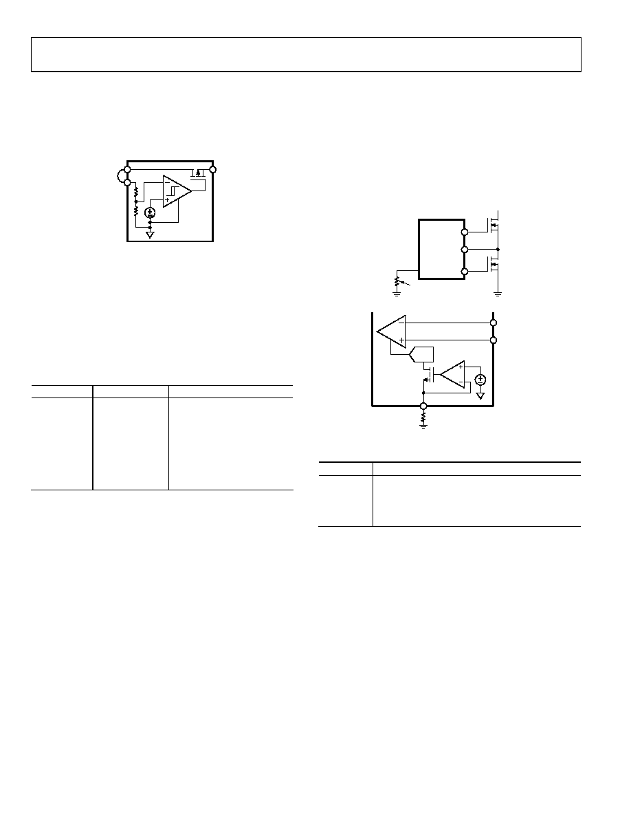
PROGRAMMING RESISTOR (RES) DETECT CIRCUIT
Upon startup, one of the first blocks to become active is the RES
detect circuit. This block powers up before soft start begins. It
forces a 0.4 V reference value at the RES pin (see Figure 68) and is
programmed to identify four possible resistor values: 47 kΩ, 22 kΩ,
open, and 100 kΩ.
The RES detect circuit digitizes the value of the resistor at the
RES pin (Pin 6). An internal ADC outputs a 2-bit digital code
that is used to program four separate gain configurations in the
current-sense amplifier (see Figure 69). Each configuration corre-
sponds to a current-sense gain (ACS) of 3 V/V, 6 V/V, 12 V/V, or
for the valley current-limit setting, which sets up the appropriate
current-sense gain for a given application and sets the compensation
necessary to achieve loop stability (see the Valley Current-Limit
Setting section and the Compensation Network section).
DRVH
DRVL
Q1
SW
Q2
RES
CS GAIN
PROGRAMMING
09
34
7-
0
66
Figure 68. Programming Resistor Location
SW
PGND
CS GAIN
SET
CS
AMP
ADC
RES
0.4V
09
34
7-
0
67
Figure 69. RES Detect Circuit for Current-Sense Gain Programming
Table 6. Current-Sense Gain Programming
Resistor
ACS
47 kΩ
3 V/V
22 kΩ
6 V/V
Open
12 V/V
100 kΩ
24 V/V
VALLEY CURRENT-LIMIT SETTING
The architecture of the ADP1874/ADP1875 is based on valley
current-mode control. The current limit is determined by three
components: the RON of the lower-side MOSFET, the current-
sense amplifier output voltage swing, and the current-sense gain.
The CS output voltage range is internally fixed at 1.4 V. The
current-sense gain is programmable via an external resistor at
the RES pin (see the Programming Resistor (RES) Detect Circuit
section). The RON of the lower-side MOSFET can vary over
temperature and usually has a positive TC (meaning that it
increases with temperature); therefore, it is recommended to
program the current-sense gain resistor based on the rated RON
of the MOSFET at 125°C.
相关PDF资料 |
PDF描述 |
|---|---|
| ADP2121ACBZ-1.85R7 | 1.222 A SWITCHING REGULATOR, 6640 kHz SWITCHING FREQ-MAX, PBGA6 |
| ADS-119MC | 1-CH 12-BIT FLASH METHOD ADC, PARALLEL ACCESS, CDIP24 |
| ADS6243IRGZT | 2-CH 14-BIT PROPRIETARY METHOD ADC, SERIAL ACCESS, PQCC48 |
| ADS6242IRGZTG4 | 2-CH 14-BIT PROPRIETARY METHOD ADC, SERIAL ACCESS, PQCC48 |
| ADS7806PB | 1-CH 12-BIT SUCCESSIVE APPROXIMATION ADC, SERIAL/PARALLEL ACCESS, PDIP28 |
相关代理商/技术参数 |
参数描述 |
|---|---|
| ADP1875ARQZ-1.0-R7 | 功能描述:IC REG CTRLR BUCK PWM CM 16-QSOP RoHS:是 类别:集成电路 (IC) >> PMIC - 稳压器 - DC DC 切换控制器 系列:- 标准包装:2,500 系列:- PWM 型:电流模式 输出数:1 频率 - 最大:500kHz 占空比:96% 电源电压:4 V ~ 36 V 降压:无 升压:是 回扫:无 反相:无 倍增器:无 除法器:无 Cuk:无 隔离:无 工作温度:-40°C ~ 125°C 封装/外壳:24-WQFN 裸露焊盘 包装:带卷 (TR) |
| ADP1876 | 制造商:AD 制造商全称:Analog Devices 功能描述:600 kHz Dual Output Synchronous Buck |
| ADP1876ACPZ-R7 | 功能描述:IC REG CTRLR BUCK PWM CM 32LFCSP RoHS:是 类别:集成电路 (IC) >> PMIC - 稳压器 - DC DC 切换控制器 系列:- 特色产品:LM3753/54 Scalable 2-Phase Synchronous Buck Controllers 标准包装:1 系列:PowerWise® PWM 型:电压模式 输出数:1 频率 - 最大:1MHz 占空比:81% 电源电压:4.5 V ~ 18 V 降压:是 升压:无 回扫:无 反相:无 倍增器:无 除法器:无 Cuk:无 隔离:无 工作温度:-5°C ~ 125°C 封装/外壳:32-WFQFN 裸露焊盘 包装:Digi-Reel® 产品目录页面:1303 (CN2011-ZH PDF) 其它名称:LM3754SQDKR |
| ADP1876-EVALZ | 功能描述:BOARD EVAL FOR ADP1876 RoHS:是 类别:编程器,开发系统 >> 评估板 - DC/DC 与 AC/DC(离线)SMPS 系列:* 标准包装:1 系列:- 主要目的:DC/DC,步降 输出及类型:1,非隔离 功率 - 输出:- 输出电压:3.3V 电流 - 输出:3A 输入电压:4.5 V ~ 28 V 稳压器拓扑结构:降压 频率 - 开关:250kHz 板类型:完全填充 已供物品:板 已用 IC / 零件:L7981 其它名称:497-12113STEVAL-ISA094V1-ND |
| ADP1877 | 制造商:AD 制造商全称:Analog Devices 功能描述:Dual Output Synchronous Buck PWM Controller With Tracking |
发布紧急采购,3分钟左右您将得到回复。