- 您现在的位置:买卖IC网 > PDF目录223311 > ADP1875ARQZ-0.3-R7 (ANALOG DEVICES INC) SWITCHING CONTROLLER, 300 kHz SWITCHING FREQ-MAX, PDSO16 PDF资料下载
参数资料
| 型号: | ADP1875ARQZ-0.3-R7 |
| 厂商: | ANALOG DEVICES INC |
| 元件分类: | 稳压器 |
| 英文描述: | SWITCHING CONTROLLER, 300 kHz SWITCHING FREQ-MAX, PDSO16 |
| 封装: | ROHS COMPLIANT, MO-137AB, QSOP-16 |
| 文件页数: | 24/44页 |
| 文件大小: | 2475K |
| 代理商: | ADP1875ARQZ-0.3-R7 |
第1页第2页第3页第4页第5页第6页第7页第8页第9页第10页第11页第12页第13页第14页第15页第16页第17页第18页第19页第20页第21页第22页第23页当前第24页第25页第26页第27页第28页第29页第30页第31页第32页第33页第34页第35页第36页第37页第38页第39页第40页第41页第42页第43页第44页
ADP1874/ADP1875
Rev. 0 | Page 30 of 44
Diode Conduction Loss
The ADP1874/ADP1875 employ anti cross-conduction circuitry
that prevents the upper- and lower-side MOSFETs from conducting
current simultaneously. This overlap control is beneficial, avoiding
large current flow that may lead to irreparable damage to the
external components of the power stage. However, this blanking
period comes with the trade-off of a diode conduction loss
occurring immediately after the MOSFET change states and
continuing well into idle mode. The amount of loss through the
body diode of the lower-side MOSFET during the anti-overlap
state is given by the following expression:
2
)
(
)
(
×
=
F
LOAD
SW
LOSS
BODY
LOSS
BODY
V
I
t
P
where:
time periods).
tSW is the period per switching cycle.
VF is the forward drop of the body diode during conduction.
(See the selected external MOSFET data sheet for more
information about the VF parameter.)
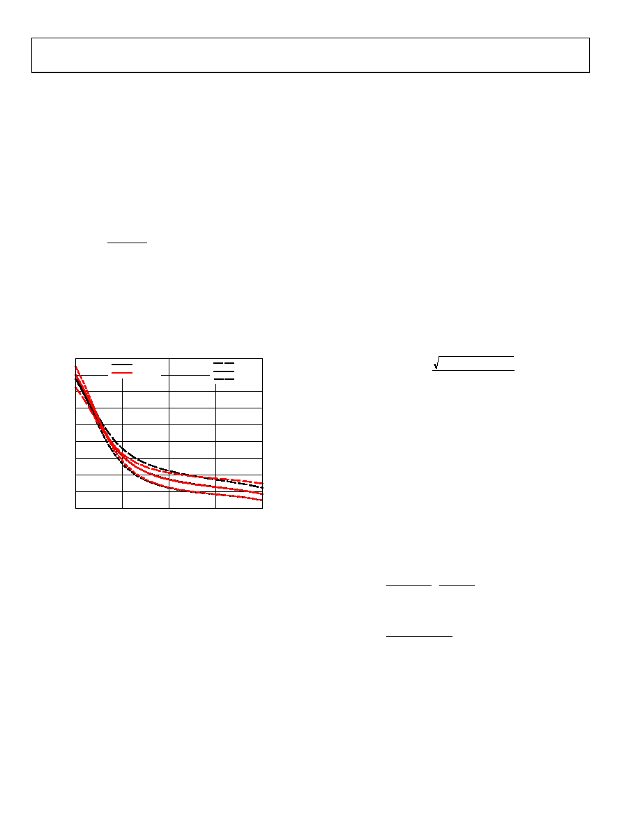
80
72
64
56
48
40
32
24
16
8
2.7
5.5
4.8
4.1
3.4
BO
DY
DI
O
D
E
CO
N
DUCT
IO
N
T
IM
E
(
n
s)
VREG (V)
+125°C
+25°C
–40°C
1MHz
300kHz
09
34
7-
08
0
Figure 88. Body Diode Conduction Time vs. Low Voltage Input (VREG)
Inductor Loss
During normal conduction mode, further power loss is caused
by the conduction of current through the inductor windings,
which have dc resistance (DCR). Typically, larger sized inductors
have smaller DCR values.
The inductor core loss is a result of the eddy currents generated
within the core material. These eddy currents are induced by the
changing flux, which is produced by the current flowing through
the windings. The amount of inductor core loss depends on the
core material, the flux swing, the frequency, and the core volume.
Ferrite inductors have the lowest core losses, whereas powdered iron
inductors have higher core losses. It is recommended to use shielded
ferrite core material type inductors with the ADP1874/ADP1875
for a high current, dc-to-dc switching application to achieve
minimal loss and negligible electromagnetic interference (EMI).
2
)
(
LOAD
LOSS
DCR
I
DCR
P
×
=
+ Core Loss
INPUT CAPACITOR SELECTION
The goal in selecting an input capacitor is to reduce or minimize
input voltage ripple and to reduce the high frequency source
impedance, which is essential for achieving predictable loop
stability and transient performance.
The problem with using bulk capacitors, other than their physical
geometries, is their large equivalent series resistance (ESR) and
large equivalent series inductance (ESL). Aluminum electrolytic
capacitors have such high ESR that they cause undesired input
voltage ripple magnitudes and are generally not effective at high
switching frequencies.
If bulk electrolytic capacitors are used, it is recommended to use
multilayered ceramic capacitors (MLCC) in parallel due to their
low ESR values. This dramatically reduces the input voltage ripple
amplitude as long as the MLCCs are mounted directly across the
drain of the upper-side MOSFET and the source terminal of the
lower-side MOSFET (see the Layout Considerations section).
Improper placement and mounting of these MLCCs may cancel
their effectiveness due to stray inductance and an increase in
trace impedance.
()
OUT
IN
OUT
MAX
LOAD
RMS
CIN
V
I
×
=
,
The maximum input voltage ripple and maximum input capacitor
rms current occur at the end of the duration of 1 D while the
upper-side MOSFET is in the off state. The input capacitor rms
current reaches its maximum at Time D. When calculating the
maximum input voltage ripple, account for the ESR of the input
capacitor as follows:
VMAX,RIPPLE = VRIPP + (ILOAD,MAX × ESR)
where:
VRIPP is usually 1% of the minimum voltage input.
ILOAD,MAX is the maximum load current.
ESR is the equivalent series resistance rating of the input capacitor.
Inserting VMAX,RIPPLE into the charge balance equation to
calculate the minimum input capacitor requirement gives
SW
RIPPLE
MAX
LOAD
IN,min
f
D
V
I
C
)
1
(
,
×
=
or
RIPPLE
MAX
SW
MAX
LOAD
IN,min
V
f
I
C
,
4
=
where D = 50%.
相关PDF资料 |
PDF描述 |
|---|---|
| ADP2121ACBZ-1.85R7 | 1.222 A SWITCHING REGULATOR, 6640 kHz SWITCHING FREQ-MAX, PBGA6 |
| ADS-119MC | 1-CH 12-BIT FLASH METHOD ADC, PARALLEL ACCESS, CDIP24 |
| ADS6243IRGZT | 2-CH 14-BIT PROPRIETARY METHOD ADC, SERIAL ACCESS, PQCC48 |
| ADS6242IRGZTG4 | 2-CH 14-BIT PROPRIETARY METHOD ADC, SERIAL ACCESS, PQCC48 |
| ADS7806PB | 1-CH 12-BIT SUCCESSIVE APPROXIMATION ADC, SERIAL/PARALLEL ACCESS, PDIP28 |
相关代理商/技术参数 |
参数描述 |
|---|---|
| ADP1875ARQZ-1.0-R7 | 功能描述:IC REG CTRLR BUCK PWM CM 16-QSOP RoHS:是 类别:集成电路 (IC) >> PMIC - 稳压器 - DC DC 切换控制器 系列:- 标准包装:2,500 系列:- PWM 型:电流模式 输出数:1 频率 - 最大:500kHz 占空比:96% 电源电压:4 V ~ 36 V 降压:无 升压:是 回扫:无 反相:无 倍增器:无 除法器:无 Cuk:无 隔离:无 工作温度:-40°C ~ 125°C 封装/外壳:24-WQFN 裸露焊盘 包装:带卷 (TR) |
| ADP1876 | 制造商:AD 制造商全称:Analog Devices 功能描述:600 kHz Dual Output Synchronous Buck |
| ADP1876ACPZ-R7 | 功能描述:IC REG CTRLR BUCK PWM CM 32LFCSP RoHS:是 类别:集成电路 (IC) >> PMIC - 稳压器 - DC DC 切换控制器 系列:- 特色产品:LM3753/54 Scalable 2-Phase Synchronous Buck Controllers 标准包装:1 系列:PowerWise® PWM 型:电压模式 输出数:1 频率 - 最大:1MHz 占空比:81% 电源电压:4.5 V ~ 18 V 降压:是 升压:无 回扫:无 反相:无 倍增器:无 除法器:无 Cuk:无 隔离:无 工作温度:-5°C ~ 125°C 封装/外壳:32-WFQFN 裸露焊盘 包装:Digi-Reel® 产品目录页面:1303 (CN2011-ZH PDF) 其它名称:LM3754SQDKR |
| ADP1876-EVALZ | 功能描述:BOARD EVAL FOR ADP1876 RoHS:是 类别:编程器,开发系统 >> 评估板 - DC/DC 与 AC/DC(离线)SMPS 系列:* 标准包装:1 系列:- 主要目的:DC/DC,步降 输出及类型:1,非隔离 功率 - 输出:- 输出电压:3.3V 电流 - 输出:3A 输入电压:4.5 V ~ 28 V 稳压器拓扑结构:降压 频率 - 开关:250kHz 板类型:完全填充 已供物品:板 已用 IC / 零件:L7981 其它名称:497-12113STEVAL-ISA094V1-ND |
| ADP1877 | 制造商:AD 制造商全称:Analog Devices 功能描述:Dual Output Synchronous Buck PWM Controller With Tracking |
发布紧急采购,3分钟左右您将得到回复。