- 您现在的位置:买卖IC网 > PDF目录15352 > ADP1879ACPZ-0.6-R7 (Analog Devices Inc)IC REG CTRLR BUCK PWM CM 14LFCSP PDF资料下载
参数资料
| 型号: | ADP1879ACPZ-0.6-R7 |
| 厂商: | Analog Devices Inc |
| 文件页数: | 18/40页 |
| 文件大小: | 0K |
| 描述: | IC REG CTRLR BUCK PWM CM 14LFCSP |
| 标准包装: | 1,500 |
| PWM 型: | 电流模式 |
| 输出数: | 1 |
| 频率 - 最大: | 600kHz |
| 占空比: | 65% |
| 电源电压: | 2.95 V ~ 20 V |
| 降压: | 是 |
| 升压: | 无 |
| 回扫: | 无 |
| 反相: | 无 |
| 倍增器: | 无 |
| 除法器: | 无 |
| Cuk: | 无 |
| 隔离: | 无 |
| 工作温度: | -40°C ~ 125°C |
| 封装/外壳: | 14-WFDFN 裸露焊盘,CSP |
| 包装: | 带卷 (TR) |
第1页第2页第3页第4页第5页第6页第7页第8页第9页第10页第11页第12页第13页第14页第15页第16页第17页当前第18页第19页第20页第21页第22页第23页第24页第25页第26页第27页第28页第29页第30页第31页第32页第33页第34页第35页第36页第37页第38页第39页第40页
�� �
�
�ADP1878/ADP1879�
�STARTUP�
�Each� ADP1878� /� ADP1879� has� an� internal� regulator� (VREG)�
�for� biasing� and� supplying� power� for� the� integrated� N-channel�
�MOSFET� drivers.� Place� a� bypass� capacitor� directly� across� the�
�VREG� (Pin� 7)� and� PGND� (Pin� 13)� pins.� Included� in� the� power-�
�up� sequence� is� the� biasing� of� the� current� sense� amplifier,� the�
��Data� Sheet�
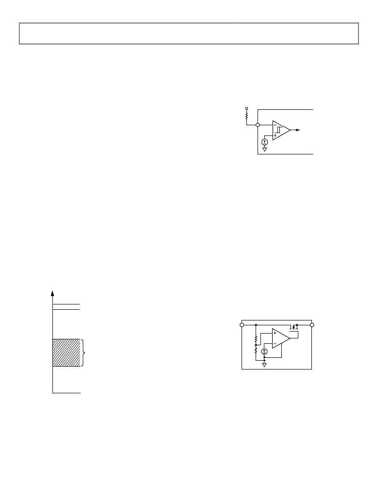
�PRECISION� ENABLE� CIRCUITRY�
�The� ADP1878� /� ADP1879� have� precision� enable� circuitry.� The�
�precision� enable� threshold� is� 630� mV� including� 30� mV� of�
�hysteresis� (see� Figure� 66).� Connecting� the� EN� pin� to� GND�
�disables� the� ADP1878� /� ADP1879� ,� reducing� the� supply� current�
�of� the� device� to� approximately� 140� μA.�
�V� REG�
��amplifier.�
�10k?�
�EN�
�PRECISION�
�ENABLE� COMP.�
�The� current� sense� blocks� provide� valley� current� information�
�(see� the� Programming� Resistor� (RES)� Detect� Circuit� section)�
�and� they� are� a� variable� of� the� compensation� equation� for� loop�
�stability� (see� the� Compensation� Network� section).� In� a� process�
�performed� by� the� RES� detect� circuit,� the� valley� current� informa-�
�tion� is� extracted� by� forcing� 0.4� V� across� the� RES� and� PGND� pins�
�generating� current.� The� current� through� the� RES� resistor� is� used�
�to� set� the� current� sense� amplifier� gain� (see� the� Programming�
��imately� 800� μs,� after� which� time� the� drive� signal� pulses� appear� at�
�the� DRVL� and� DRVH� pins� synchronously,� and� the� output� voltage�
�begins� to� rise� in� a� controlled� manner� through� the� soft� start�
�sequence.�
�The� soft� start� and� error� amplifier� blocks� determine� the� rise� time�
�of� the� output� voltage� (see� the� Soft� Start� section).� At� the� beginning�
�of� a� soft� start,� the� error� amplifier� charges� the� external� compensa-�
��Tying� the� VREG� pin� to� the� EN� pin� via� a� pull-up� resistor� causes�
�the� voltage� at� the� EN� pin� to� rise� above� the� enable� threshold� of�
��COMP�
�TO� ENABLE�
�ALL� BLOCKS�
�630mV�
�Figure� 66.� Connecting� EN� Pin� to� VREG� via� a� Pull-Up� Resistor� to� Enable� the�
��UNDERVOLTAGE� LOCKOUT�
�The� undervoltage� lockout� (UVLO)� feature� prevents� the� device�
�from� operating� both� the� high-� and� low-side� N-channel� MOSFETs�
�at� extremely� low� or� undefined� input� voltage� (V� IN� )� ranges.�
�Operation� at� an� undefined� bias� voltage� can� result� in� the�
�incorrect� propagation� of� signals� to� the� high-side� power� switches.�
�This,� in� turn,� results� in� invalid� output� behavior� that� can� cause�
�damage� to� the� output� devices,� ultimately� destroying� the� device�
�tied� at� the� output.� The� UVLO� level� is� set� at� 2.65� V� (nominal).�
�ON-BOARD� LOW� DROPOUT� (LDO)� REGULATOR�
�The� ADP1878� /� ADP1879� use� an� on-board� LDO� to� bias� the�
�internal� digital� and� analog� circuitry.� With� proper� bypass�
�capacitors� connected� to� the� VREG� pin� (output� of� the� internal�
�LDO),� this� pin� also� provides� power� for� the� internal� MOSFET�
�drivers.� It� is� recommended� to� float� VREG� if� VIN� is� used� for�
�>2.4V�
�2.4V�
�1.0V�
�500mV�
�HICCUP� MODE� INITIALIZED�
�MAXIMUM� CURRENT� (UPPER� CLAMP)�
�ZERO� CURRENT�
�USABLE� RANGE� ONLY� AFTER� SOFT� START�
�PERIOD� IF� CONTINUOUS� CONDUCTION�
�MODE� OF� OPERATION� IS� SELECTED.�
�LOWER� CLAMP�
�greater� than� 5.5� V� operation.� The� minimum� voltage� at� which�
��ON-BOARD� REGULATOR�
�VREG�
�VIN�
�REF�
�Figure� 67.� On-Board� Regulator�
�For� applications� where� VIN� is� decoupled� from� VREG,� the�
�0V�
�Figure� 65.� COMP� Voltage� Range�
�minimum� voltage� at� VIN� must� be� 2.9� V.� It� is� recommended� to� tie�
�VIN� and� VREG� together� if� the� VIN� pin� is� subjected� to� a� 2.75� V� rail.�
�SOFT� START�
�The� ADP1878� employs� externally� programmable,� soft� start�
�circuitry� that� charges� up� a� capacitor� tied� to� the� SS� pin� to� GND.�
�This� prevents� input� inrush� current� through� the� external� MOSFET�
�from� the� input� supply� (V� IN� ).� The� output� tracks� the� ramping� voltage�
�by� producing� PWM� output� pulses� to� the� high-side� MOSFET.� The�
�purpose� is� to� limit� the� inrush� current� from� the� high� voltage�
�input� supply� (V� IN� )� to� the� output� (V� OUT� ).�
�Rev.� B� |� Page� 18� of� 40�
�相关PDF资料 |
PDF描述 |
|---|---|
| EBC49DRXH-S734 | CONN EDGECARD 98POS DIP .100 SLD |
| VE-2WN-EY-F3 | CONVERTER MOD DC/DC 18.5V 50W |
| VI-B1F-EV-F2 | CONVERTER MOD DC/DC 72V 150W |
| ADP1879ACPZ-1.0-R7 | IC REG CTRLR BUCK PWM CM 14LFCSP |
| VE-2WN-EY-F2 | CONVERTER MOD DC/DC 18.5V 50W |
相关代理商/技术参数 |
参数描述 |
|---|---|
| ADP1879ACPZ-1.0-R7 | 功能描述:IC REG CTRLR BUCK PWM CM 14LFCSP RoHS:是 类别:集成电路 (IC) >> PMIC - 稳压器 - DC DC 切换控制器 系列:- 标准包装:2,500 系列:- PWM 型:电流模式 输出数:1 频率 - 最大:500kHz 占空比:96% 电源电压:4 V ~ 36 V 降压:无 升压:是 回扫:无 反相:无 倍增器:无 除法器:无 Cuk:无 隔离:无 工作温度:-40°C ~ 125°C 封装/外壳:24-WQFN 裸露焊盘 包装:带卷 (TR) |
| ADP1880ACPZ-R7 | 制造商:Analog Devices 功能描述: |
| ADP1882 | 制造商:AD 制造商全称:Analog Devices 功能描述:Synchronous Current-Mode with Constant On-Time,PWM Buck Controller |
| ADP1882-0.3-EVALZ | 功能描述:EVAL BOARD FOR ADP1882 RoHS:是 类别:编程器,开发系统 >> 评估板 - DC/DC 与 AC/DC(离线)SMPS 系列:- 产品培训模块:Obsolescence Mitigation Program 标准包装:1 系列:True Shutdown™ 主要目的:DC/DC,步升 输出及类型:1,非隔离 功率 - 输出:- 输出电压:- 电流 - 输出:1A 输入电压:2.5 V ~ 5.5 V 稳压器拓扑结构:升压 频率 - 开关:3MHz 板类型:完全填充 已供物品:板 已用 IC / 零件:MAX8969 |
| ADP1882-0.6-EVALZ | 功能描述:EVAL BOARD FOR ADP1882 RoHS:是 类别:编程器,开发系统 >> 评估板 - DC/DC 与 AC/DC(离线)SMPS 系列:- 产品培训模块:Obsolescence Mitigation Program 标准包装:1 系列:True Shutdown™ 主要目的:DC/DC,步升 输出及类型:1,非隔离 功率 - 输出:- 输出电压:- 电流 - 输出:1A 输入电压:2.5 V ~ 5.5 V 稳压器拓扑结构:升压 频率 - 开关:3MHz 板类型:完全填充 已供物品:板 已用 IC / 零件:MAX8969 |
发布紧急采购,3分钟左右您将得到回复。