- 您现在的位置:买卖IC网 > PDF目录20615 > ADP191ACBZ-R7 (Analog Devices Inc)IC CTLR HIGH LSIDE PWR SW 4WLCSP PDF资料下载
参数资料
| 型号: | ADP191ACBZ-R7 |
| 厂商: | Analog Devices Inc |
| 文件页数: | 12/16页 |
| 文件大小: | 0K |
| 描述: | IC CTLR HIGH LSIDE PWR SW 4WLCSP |
| 产品变化通告: | 8mm Carrier Tape Changes 28/Feb/2012 |
| 标准包装: | 1 |
| 类型: | 高端开关 |
| 导通状态电阻: | 105 毫欧 |
| 电源电压: | 1.1 V ~ 3.6 V |
| 工作温度: | -40°C ~ 85°C |
| 安装类型: | 表面贴装 |
| 封装/外壳: | 4-WFBGA,WLCSP |
| 供应商设备封装: | 4-WLCSP(0.76x0.76) |
| 包装: | 标准包装 |
| 配用: | ADP191CB-EVALZ-ND - EVAL BOARD FOR ADP191 |
| 其它名称: | ADP191ACBZ-R7DKR |
�� �
�
�ADP190/ADP191�
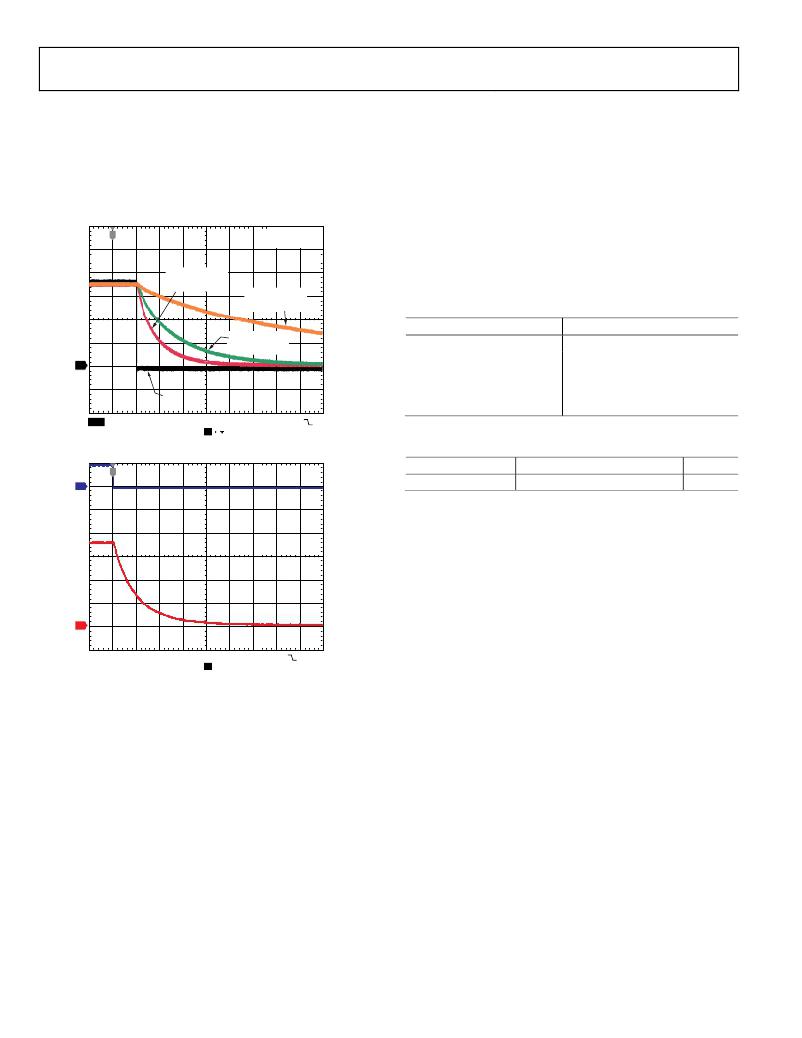
�The� turn-off� time� is� defined� as� the� delta� between� the� time� from�
�90%� to� 10%� of� VOUT� reaching� its� final� value.� It� is� also� dependent�
�on� the� RC� time� constant.�
�The� ADP191� incorporates� an� internal� output� discharge� resistor�
�to� discharge� the� output� capacitance� when� the� ADP191� output� is�
�disabled.� See� Figure� 28� and� Figure� 29� for� a� comparison� of� turn-�
�off� times.�
�T� V� OUT� =� 1.8V�
�V� EN� =� 3.6V�
�Data� Sheet�
�To� guarantee� reliable� operation,� the� junction� temperature� of�
�the� ADP190� /� ADP191� must� not� exceed� 125°C.� To� ensure� that�
�the� junction� temperature� stays� below� this� maximum� value,� the�
�user� must� be� aware� of� the� parameters� that� contribute� to� junction�
�temperature� changes.� These� parameters� include� ambient� temper-�
�ature,� power� dissipation� in� the� power� device,� and� thermal�
�resistances� between� the� junction� and� ambient� air� (θ� JA� ).� The� θ� JA�
�value� is� dependent� on� the� package� assembly� compounds� that�
�are� used� and� the� amount� of� copper� used� to� solder� the� package�
�GND� pin� to� the� PCB.� Table� 6� shows� typical� θ� JA� values� of� the� 4-ball�
�I� LOAD� =� 200mA,�
�C� LOAD� =� 1μF�
�I� LOAD� =� 100mA,�
�C� LOAD� =� 4.7μF�
�WLCSP� for� various� PCB� copper� sizes.� Table� 7� shows� the� typical�
�Ψ� JB� value� of� the� 4-ball� WLCSP.�
�Table� 6.� Typical� θ� JA� Values� for� WLCSP�
�Copper� Size� (mm� 2� )�
�θ� JA� (°C/W)�
�1� 2�
�V� EN�
�I� LOAD� =� 100mA,�
�C� LOAD� =� 1μF�
��50�
�100�
�300�
�500�
�260�
�159�
�157�
�153�
�151�
�CH1� 1V�
�CH2� 500mV�
�M10μs�
�T� 30.36μs�
�A� CH1�
�1V�
�1�
�Device� soldered� to� minimum� size� pin� traces.�
�Figure� 28.� ADP190� Typical� Turn-Off� Time,� Various� Load� Currents�
�Table� 7.� Typical� Ψ� JB� Values�
�1�
�T�
�V� EN�
�Package�
�4-Ball� WLCSP�
�Ψ� JB�
�58.4�
�Unit�
�°C/W�
�The� junction� temperature� of� the� ADP190� /� ADP191� can� be�
�calculated� from� the� following� equation:�
�T� J� =� T� A� +� (� P� D� ×� θ� JA� )�
�where:�
�T� A� is� the� ambient� temperature.�
�P� D� is� the� power� dissipation� in� the� die,� given� by�
�(1)�
�3�
�V� OUT�
�P� D� =� [(� V� IN� ?� V� OUT� )� � I� LOAD� ]� +� (� V� IN� � I� GND� )�
�(2)�
�CH1� 2.00V� M200μs� A� CH1� 600mV�
�CH3� 500mV� T� 10.20%�
�Figure� 29.� ADP191� Typical� Turn-Off� Time,� Load� Current� =� 0� mA�
�THERMAL� CONSIDERATIONS�
�In� most� applications,� the� ADP190� /� ADP191� do� not� dissipate�
�much� heat� due� to� their� low� on-channel� resistance.� However,� in�
�applications� with� high� ambient� temperature� and� load� current,�
�the� heat� dissipated� in� the� package� can� be� large� enough� to� cause�
�the� junction� temperature� of� the� die� to� exceed� the� maximum�
�junction� temperature� of� 125°C.�
�The� junction� temperature� of� the� die� is� the� sum� of� the� ambient�
�temperature� of� the� environment� and� the� temperature� rise� of� the�
�package� due� to� the� power� dissipation,� as� shown� in� Equation� 1.�
�where:�
�I� LOAD� is� the� load� current.�
�I� GND� is� the� ground� current.�
�V� IN� and� V� OUT� are� the� input� and� output� voltages,� respectively.�
�Power� dissipation� due� to� ground� current� is� quite� small� and�
�can� be� ignored.� Therefore,� the� junction� temperature� equation�
�simplifies� to� the� following:�
�T� J� =� T� A� +� {[(� V� IN� ?� V� OUT� )� ×� I� LOAD� ]� ×� θ� JA� }� (3)�
�As� shown� in� Equation� 3,� for� a� given� ambient� temperature,� input-�
�to-output� voltage� differential,� and� continuous� load� current,� there�
�exists� a� minimum� copper� size� requirement� for� the� PCB� to� ensure�
��to� Figure� 35� show� junction� temperature� calculations� for� different�
�ambient� temperatures,� load� currents,� V� IN� to� V� OUT� differentials,�
�and� areas� of� PCB� copper.�
�Rev.� E� |� Page� 12� of� 16�
�相关PDF资料 |
PDF描述 |
|---|---|
| 591D476X0010R2T15H | CAP TANT 47UF 10V 20% 2824 |
| VI-BNP-EU-F3 | CONVERTER MOD DC/DC 13.8V 200W |
| ESC60DRYS | CONN EDGECARD 120PS DIP .100 SLD |
| VI-BNL-EU-F2 | CONVERTER MOD DC/DC 28V 200W |
| TTN2.50SV50 | THERMASHIELD TUBE 2 1/2" SLV 50' |
相关代理商/技术参数 |
参数描述 |
|---|---|
| ADP191CB-EVALZ | 功能描述:EVAL BOARD FOR ADP191 RoHS:是 类别:编程器,开发系统 >> 评估演示板和套件 系列:- 标准包装:1 系列:- 主要目的:电信,线路接口单元(LIU) 嵌入式:- 已用 IC / 零件:IDT82V2081 主要属性:T1/J1/E1 LIU 次要属性:- 已供物品:板,电源,线缆,CD 其它名称:82EBV2081 |
| ADP194 | 制造商:AD 制造商全称:Analog Devices 功能描述:Logic Controlled, High-Side Power Switch Low RDSON of 80 mΩ at 1.8 V |
| ADP194ACBZ-R7 | 功能描述:IC POWER SWITCH HS LOGIC 4WLSCP RoHS:是 类别:集成电路 (IC) >> PMIC - MOSFET,电桥驱动器 - 内部开关 系列:- 标准包装:2,500 系列:- 类型:高端 输入类型:非反相 输出数:1 导通状态电阻:35 毫欧 电流 - 输出 / 通道:- 电流 - 峰值输出:3A 电源电压:2.7 V ~ 5.5 V 工作温度:-40°C ~ 85°C 安装类型:表面贴装 封装/外壳:14-TSSOP(0.173",4.40mm 宽) 供应商设备封装:14-TSSOP 包装:带卷 (TR) 其它名称:MIC2545A-1YTSTRMIC2545A-1YTSTR-ND |
| ADP194CB-EVALZ | 功能描述:BOARD EVAL FOR ADP194ACBZ RoHS:是 类别:编程器,开发系统 >> 评估演示板和套件 系列:* 标准包装:1 系列:- 主要目的:电信,线路接口单元(LIU) 嵌入式:- 已用 IC / 零件:IDT82V2081 主要属性:T1/J1/E1 LIU 次要属性:- 已供物品:板,电源,线缆,CD 其它名称:82EBV2081 |
| ADP195 | 制造商:AD 制造商全称:Analog Devices 功能描述:Logic Controlled, High-Side Power Switch with Reverse Current Blocking |
发布紧急采购,3分钟左右您将得到回复。