- 您现在的位置:买卖IC网 > PDF目录13140 > ADP3334ARMZ-REEL7 (Analog Devices Inc)IC REG LDO ADJ .5A 8MSOP PDF资料下载
参数资料
| 型号: | ADP3334ARMZ-REEL7 |
| 厂商: | Analog Devices Inc |
| 文件页数: | 8/11页 |
| 文件大小: | 0K |
| 描述: | IC REG LDO ADJ .5A 8MSOP |
| 设计资源: | Broadband Low EVM Direct Conversion Transmitter (CN0134) Broadband Low EVM Direct Conversion Transmitter Using LO Divide-by-2 Modulator (CN0144) |
| 标准包装: | 1 |
| 系列: | anyCAP® |
| 稳压器拓扑结构: | 正,可调式 |
| 输出电压: | 1.5 V ~ 10 V |
| 输入电压: | 2.6 V ~ 11 V |
| 电压 - 压降(标准): | 0.2V @ 500mA |
| 稳压器数量: | 1 |
| 电流 - 输出: | 500mA |
| 工作温度: | -40°C ~ 85°C |
| 安装类型: | 表面贴装 |
| 封装/外壳: | 8-TSSOP,8-MSOP(0.118",3.00mm 宽) |
| 供应商设备封装: | 8-MSOP |
| 包装: | 标准包装 |
| 其它名称: | ADP3334ARMZ-REEL7DKR |
�� �
�
�ADP3334�
�P� D� =� (� V� IN� -� V� OUT� )� I� LOAD� +� (� V� IN� )� I� GND�
�Current� and� thermal� limit� protections� are� intended� to� protect�
�the� device� against� accidental� overload� conditions.� For� normal�
�operation,� device� power� dissipation� should� be� externally� limited�
�so� that� junction� temperatures� will� not� exceed� 150°C.�
�Calculating� Junction� Temperature�
�Device� power� dissipation� is� calculated� as� follows:�
�(8)�
�where� I� LOAD� and� I� GND� are� load� current� and� ground� current,� V� IN�
�and� V� OUT� are� input� and� output� voltages,� respectively.�
�Assuming� I� LOAD� =� 400� mA� ,� I� GND� =� 4� mA� ,� V� IN� =� 5.0� V� and�
�As� an� example,� the� patented� thermal� coastline� lead� frame� design�
�of� the� ADP3334� uniformly� minimizes� the� value� of� the� dominant�
�portion� of� the� thermal� resistance.� It� ensures� that� heat� is� con-�
�ducted� away� by� all� pins� of� the� package.� This� yields� a� very� low�
�86.6°C/W� thermal� resistance� for� the� SOIC-8� package,� without�
�any� special� board� layout� requirements,� relying� only� on� the� normal�
�traces� connected� to� the� leads.� This� yields� a� 15%� improvement� in�
�heat� dissipation� capability� as� compared� to� a� standard� SOIC-8�
�package.� The� thermal� resistance� can� be� decreased� by� an� addi-�
�tional� 10%� by� attaching� a� few� square� centimeters� of� copper� area�
�to� the� IN� or� OUT� pins� of� the� ADP3334� package.�
�V� OUT� =� 2.8� V� ,� device� power� dissipation� is:�
�P� D� =� (� 5� -� 2� .� 8� )� 400� mA� +� 5� .� 0� (� 4� mA� )� =� 900� mW�
�(9)�
�It� is� not� recommended� to� use� solder� mask� or� silkscreen� on� the�
�PCB� traces� adjacent� to� the� ADP3334’s� pins� since� it� will� increase�
�the� junction-to-ambient� thermal� resistance� of� the� package.�
�As� an� example,� the� proprietary� package� used� in� the� ADP3334�
�has� a� thermal� resistance� of� 86.6°C/W,� significantly� lower� than�
�a� standard� SOIC-8� package.� Assuming� a� 4-layer� board,� the�
�junction� temperature� rise� above� ambient� temperature� will� be�
�approximately� equal� to:�
�2x� VIAS,� 0.250�
�35μm� PLATING�
�0.73�
�0.30�
�D� T� J� A� =� 0� .� 900� W� ¥� 86� .� 6� ∞� C� /� W� =� 77� .� 9� ∞� C�
�(10)�
�1.80�
�To� limit� the� maximum� junction� temperature� to� 150°C,� maxi-�
�mum� allowable� ambient� temperature� will� be:�
�T� AMAX� =� 150� ∞� C� -� 77� .� 9� ∞� C� /� W� =� 72� .� 1� ∞� C�
�(11)�
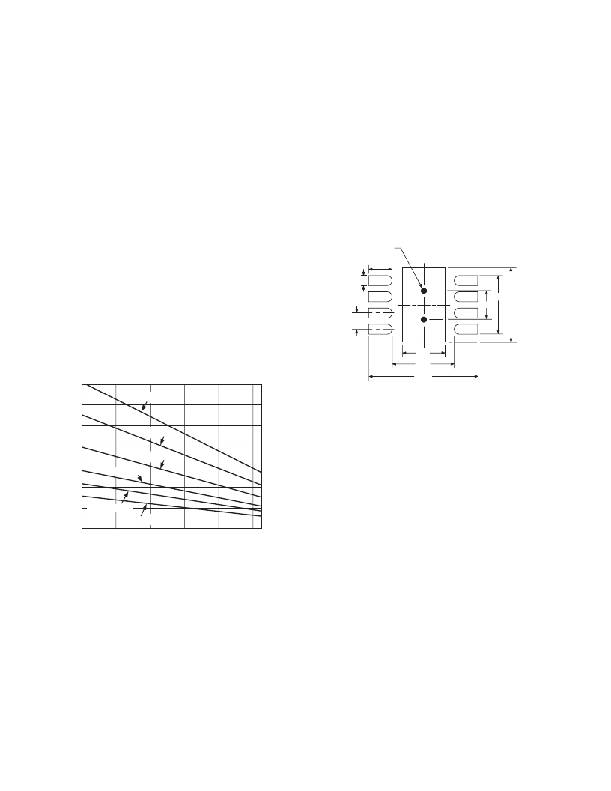
�The� maximum� power� dissipation� versus� ambient� temperature�
�for� each� package� is� shown� in� Figure� 5.�
�0.50�
�1.40�
�1.90�
�0.90�
�2.36�
�3.36�
�3.5�
�3.0�
�2.5�
�2.0�
�1.5�
�1.0�
�0.5�
�0�
�48� C/W� LFCSP�
�62� C/W� LFCSP�
�86� C/W� SOIC�
�122� C/W� SOIC�
�158 C/W MSOP�
�220� C/W� MSOP�
�Figure� 6.� 3� mm� x� 3� mm� LFCSP� Pad� Pattern�
�(Dimensions� shown� in� millimeters)�
�LFCSP� Layout� Considerations�
�The� LFCSP� package� has� an� exposed� die� paddle� on� the� bottom,�
�which� efficiently� conducts� heat� to� the� PCB.� In� order� to� achieve�
�the� optimum� performance� from� the� LFCSP� package,� special�
�consideration� must� be� given� to� the� layout� of� the� PCB.� Use� the�
�following� layout� guidelines� for� the� LFCSP� package.�
�1.� The� pad� pattern� is� given� in� Figure� 6.� The� pad� dimension�
�should� be� followed� closely� for� reliable� solder� joints� while�
�maintaining� reasonable� clearances� to� prevent� solder� bridging.�
�2.� The� thermal� pad� of� the� LFCSP� package� provides� a� low� ther-�
�–20�
�0�
�20� 40�
�60�
�80�
�mal� impedance� path� (approximately� 20°C/W)� to� the� PCB.�
�AMBIENT� TEMPERATURE� –� C�
�Figure� 5.� Power� Derating� Curve�
�Printed� Circuit� Board� Layout� Consideration�
�All� surface-mount� packages� rely� on� the� traces� of� the� PC� board�
�to� conduct� heat� away� from� the� package.�
�In� standard� packages,� the� dominant� component� of� the� heat�
�resistance� path� is� the� plastic� between� the� die� attach� pad� and� the�
�individual� leads.� In� typical� thermally� enhanced� packages,� one� or�
�more� of� the� leads� are� fused� to� the� die� attach� pad,� significantly�
�decreasing� this� component.� To� make� the� improvement� mean-�
�ingful,� however,� a� significant� copper� area� on� the� PCB� must� be�
�attached� to� these� fused� pins.�
�–8� –�
�Therefore� the� PCB� must� be� properly� designed� to� effectively�
�conduct� the� heat� away� from� the� package.� This� is� achieved� by�
�adding� thermal� vias� to� the� PCB,� which� provide� a� thermal�
�path� to� the� inner� or� bottom� layers.� See� Figure� 5� for� the� rec-�
�ommended� via� pattern.� Note� that� the� via� diameter� is� small� to�
�prevent� the� solder� from� flowing� through� the� via� and� leaving�
�voids� in� the� thermal� pad� solder� joint.�
�Note� that� the� thermal� pad� is� attached� to� the� die� substrate,� so�
�the� thermal� planes� that� the� vias� attach� the� package� to� must�
�be� electrically� isolated� or� connected� to� V� IN� .� Do� NOT� con-�
�nect� the� thermal� pad� to� ground.�
�REV.� C�
�相关PDF资料 |
PDF描述 |
|---|---|
| HCC26DRTH-S93 | CONN EDGECARD 52POS DIP .100 SLD |
| GCC43DRXS-S734 | CONN EDGECARD 86POS DIP .100 SLD |
| VI-BNF-EU | CONVERTER MOD DC/DC 72V 200W |
| VI-J6M-EX-F3 | CONVERTER MOD DC/DC 10V 75W |
| MIC5319YML TR | IC REG LDO ADJ .5A 6MLF |
相关代理商/技术参数 |
参数描述 |
|---|---|
| ADP3334AR-REEL | 制造商:Analog Devices 功能描述:LDO Regulator Pos 1.5V to 10V 0.8A 8-Pin SOIC N T/R 制造商:Rochester Electronics LLC 功能描述:500 MA ADJUSTABLE ANYCAP LDO - Tape and Reel |
| ADP3334AR-REEL7 | 制造商:Analog Devices 功能描述:LDO Regulator Pos 1.5V to 10V 0.8A 8-Pin SOIC N T/R 制造商:Rochester Electronics LLC 功能描述:500 MA ADJUSTABLE ANYCAP LDO - Tape and Reel |
| ADP3334ARZ | 功能描述:IC REG LDO ADJ .5A 8-SOIC RoHS:是 类别:集成电路 (IC) >> PMIC - 稳压器 - 线性 系列:anyCAP® 标准包装:3,000 系列:- 稳压器拓扑结构:正,固定式 输出电压:3V 输入电压:最高 5.5V 电压 - 压降(标准):0.12V @ 150mA 稳压器数量:1 电流 - 输出:150mA(最小值) 电流 - 限制(最小):220mA 工作温度:-40°C ~ 125°C 安装类型:表面贴装 封装/外壳:SOT-23-5 细型,TSOT-23-5 供应商设备封装:TSOT-23-5 包装:带卷 (TR) 其它名称:ADP160AUJZ-3.0-R7TR |
| ADP3334ARZ | 制造商:Analog Devices 功能描述:Linear Voltage Regulator IC 制造商:Analog Devices 功能描述:IC, ADJ LDO REG, 1.5V TO 10V 0.5A 8-SOIC |
| ADP3334ARZ-REEL | 功能描述:IC REG LDO ADJ .5A 8SOIC RoHS:是 类别:集成电路 (IC) >> PMIC - 稳压器 - 线性 系列:anyCAP® 标准包装:75 系列:- 稳压器拓扑结构:正,可调式 输出电压:1.2 V ~ 37 V 输入电压:4.2 V ~ 40 V 电压 - 压降(标准):- 稳压器数量:1 电流 - 输出:500mA 电流 - 限制(最小):500mA 工作温度:-40°C ~ 125°C 安装类型:表面贴装 封装/外壳:TO-252-3,DPak(2 引线+接片),SC-63 供应商设备封装:TO-252-3 包装:管件 产品目录页面:1286 (CN2011-ZH PDF) 其它名称:*LM317AMDT/NOPBLM317AMDT |
发布紧急采购,3分钟左右您将得到回复。