- 您现在的位置:买卖IC网 > PDF目录1899 > ADSP-2104BPZ-80 (Analog Devices Inc)IC DSP CONTROLLER 16BIT 68PLCC PDF资料下载
参数资料
| 型号: | ADSP-2104BPZ-80 |
| 厂商: | Analog Devices Inc |
| 文件页数: | 10/36页 |
| 文件大小: | 0K |
| 描述: | IC DSP CONTROLLER 16BIT 68PLCC |
| 产品变化通告: | Product Discontinuance 27/Oct/2011 |
| 标准包装: | 19 |
| 系列: | ADSP-21xx |
| 类型: | 定点 |
| 接口: | 同步串行端口(SSP) |
| 时钟速率: | 20MHz |
| 非易失内存: | 外部 |
| 芯片上RAM: | 1.5kB |
| 电压 - 输入/输出: | 5.00V |
| 电压 - 核心: | 5.00V |
| 工作温度: | -40°C ~ 85°C |
| 安装类型: | 表面贴装 |
| 封装/外壳: | 68-LCC(J 形引线) |
| 供应商设备封装: | 68-PLCC(24.23x24.23) |
| 包装: | 管件 |
第1页第2页第3页第4页第5页第6页第7页第8页第9页当前第10页第11页第12页第13页第14页第15页第16页第17页第18页第19页第20页第21页第22页第23页第24页第25页第26页第27页第28页第29页第30页第31页第32页第33页第34页第35页第36页
ADSP-2104/ADSP-2109
–18–
REV. 0
SPECIFICATIONS (ADSP-2104L /ADSP-2109L)
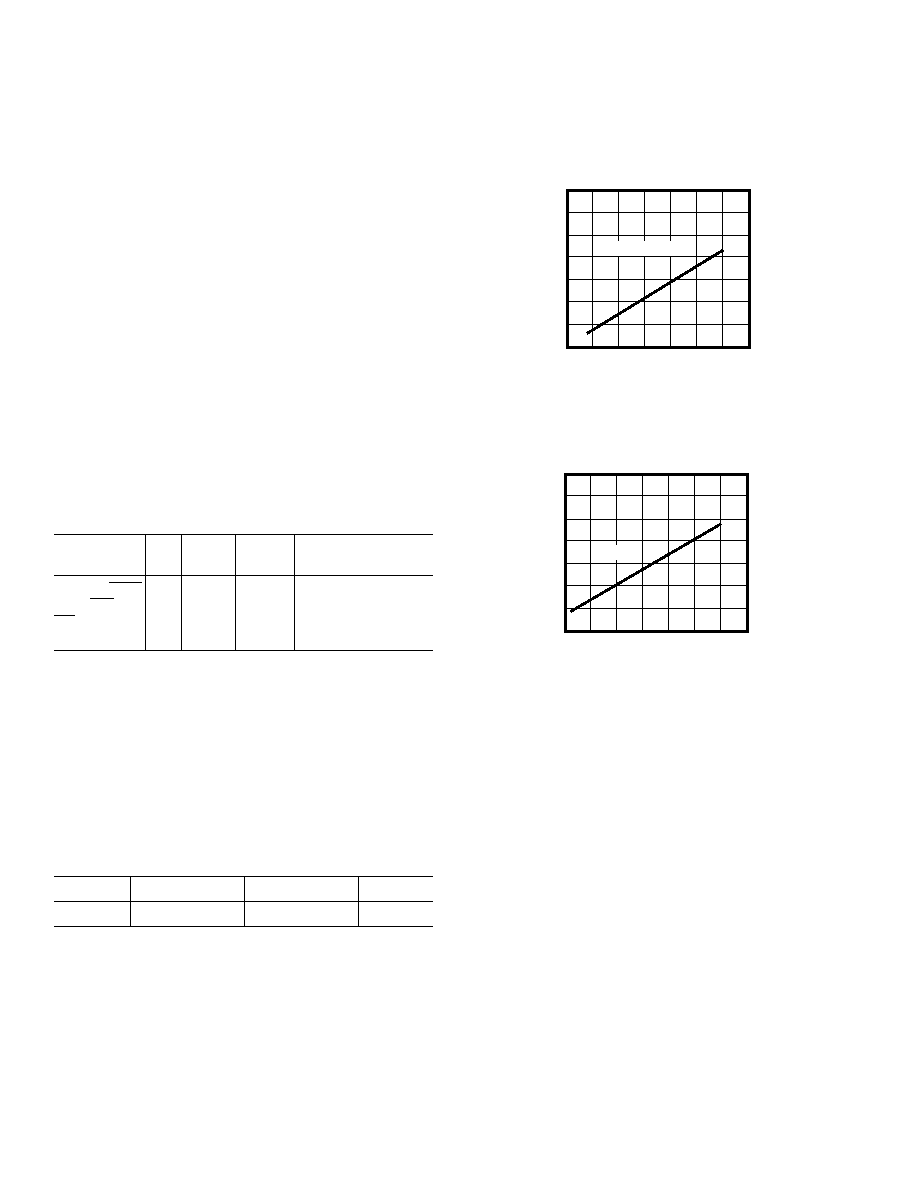
CAPACITIVE LOADING
Figures 14 and 15 show capacitive loading characteristics.
POWER DISSIPATION EXAMPLE
To determine total power dissipation in a specific application,
the following equation should be applied for each output:
C
× V
DD
2
× f
C = load capacitance, f = output switching frequency.
Example:
In an ADSP-2104L application where external data memory is
used and no other outputs are active, power dissipation is
calculated as follows:
Assumptions:
External data memory is accessed every cycle with 50% of the
address pins switching.
External data memory writes occur every other cycle with
50% of the data pins switching.
Each address and data pin has a 10 pF total load at the pin.
The application operates at V
DD = 3.3 V and tCK = 100 ns.
Total Power Dissipation = PINT + (C
× V
DD
2
× f)
PINT = internal power dissipation (from Figure 13).
(C
× V
DD
2
× f ) is calculated for each output:
# of
Output
Pins
× C
VDD
2
f
Address, DMS 8
× 10 pF × 3.32 V × 10 MHz = 8.71 mW
Data, WR
9
× 10 pF × 3.32 V × 5 MHz = 4.90 mW
RD
1
× 10 pF × 3.32 V × 5 MHz = 0.55 mW
CLKOUT
1
× 10 pF × 3.32 V × 10 MHz = 1.09 mW
15.25 mW
Total power dissipation for this example = PINT + 15.25 mW.
ENVIRONMENTAL CONDITIONS
Ambient Temperature Rating:
TAMB = TCASE – (PD × θCA)
TCASE = Case Temperature in
°C
PD = Power Dissipation in W
θ
CA = Thermal Resistance (Case-to-Ambient)
θ
JA = Thermal Resistance (Junction-to-Ambient)
θ
JC = Thermal Resistance (Junction-to-Case)
Package
JA
JC
CA
PLCC
27
°C/W
16
°C/W
11
°C/W
Figure 14. Typical Output Rise Time vs. Load Capacitance, C
L
(at Maximum Ambient Operating Temperature)
Figure 15. Typical Output Valid Delay or Hold vs. Load
Capacitance, C
L (at Maximum Ambient Operating Temperature)
25
150
125
100
75
CL – pF
50
RISE
TIME
(0.8V-2.0V)
–
ns
30
10
5
15
20
25
VDD = 3.0V
VALID
OUTPUT
DELAY
OR
HOLD
–
ns
–2
+4
+2
+6
NOMINAL
25
150
125
100
75
50
+8
VDD = 3.0V
CL – pF
相关PDF资料 |
PDF描述 |
|---|---|
| ADSP-21060LCW-160 | IC DSP CONTROLLER 32BIT 240CQFP |
| ADSP-21061KS-200 | IC DSP CONTROLLER 32BIT 240MQFP |
| ADSP-21065LCCA-240 | IC DSP CTLR 32BIT 196CSPBGA |
| ADSP-2111BG-80 | IC DSP CONTROLLER 16BIT 100PGA |
| ADSP-21160MKB-80 | IC DSP CONTROLLER 32BIT 400 BGA |
相关代理商/技术参数 |
参数描述 |
|---|---|
| ADSP-2104KP-80 | 制造商:Analog Devices 功能描述:DSP Fixed-Point 16-Bit 20MHz 20MIPS 68-Pin PLCC 制造商:Rochester Electronics LLC 功能描述:- Bulk 制造商:Analog Devices 功能描述:Low cost DSP microcomputer 1 timer 4.5 |
| ADSP-2104L | 制造商:未知厂家 制造商全称:未知厂家 功能描述:ADSP-2104/ADSP-2104L: Low Cost DSP Microcomputers Data Sheet (Rev. 0. 7/96) |
| ADSP-2104LKP-55 | 制造商:Rochester Electronics LLC 功能描述:- Bulk 制造商:Analog Devices 功能描述: |
| ADSP2105 | 制造商:未知厂家 制造商全称:未知厂家 功能描述:(666.40 k) |
| ADSP-2105 | 制造商:AD 制造商全称:Analog Devices 功能描述:ADSP-2100 Family DSP Microcomputers |
发布紧急采购,3分钟左右您将得到回复。