- 您现在的位置:买卖IC网 > PDF目录1900 > ADSP-21990BSTZ (Analog Devices Inc)IC DSP CONTROLLER 16BIT 176-LQFP PDF资料下载
参数资料
| 型号: | ADSP-21990BSTZ |
| 厂商: | Analog Devices Inc |
| 文件页数: | 34/50页 |
| 文件大小: | 0K |
| 描述: | IC DSP CONTROLLER 16BIT 176-LQFP |
| 产品变化通告: | Product Discontinuance 27/Oct/2011 |
| 标准包装: | 1 |
| 系列: | ADSP-21xx |
| 类型: | 定点 |
| 接口: | SPI,SSP |
| 时钟速率: | 160MHz |
| 非易失内存: | 外部 |
| 芯片上RAM: | 20kB |
| 电压 - 输入/输出: | 3.30V |
| 电压 - 核心: | 2.50V |
| 工作温度: | -40°C ~ 85°C |
| 安装类型: | 表面贴装 |
| 封装/外壳: | 176-LQFP |
| 供应商设备封装: | 176-LQFP(24x24) |
| 包装: | 托盘 |
第1页第2页第3页第4页第5页第6页第7页第8页第9页第10页第11页第12页第13页第14页第15页第16页第17页第18页第19页第20页第21页第22页第23页第24页第25页第26页第27页第28页第29页第30页第31页第32页第33页当前第34页第35页第36页第37页第38页第39页第40页第41页第42页第43页第44页第45页第46页第47页第48页第49页第50页
Rev. A
|
Page 4 of 50
|
August 2007
ADSP-21990
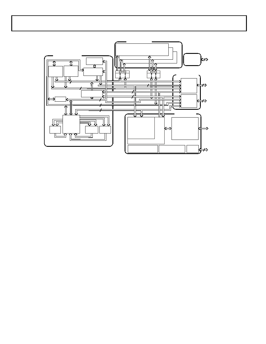
The block diagram (Figure 2) shows the architecture of the
embedded ADSP-21xx core. It contains three independent com-
putational units: the ALU, the multiplier/accumulator (MAC),
and the shifter. The computational units process 16-bit data
from the register file and have provisions to support multipreci-
sion computations. The ALU performs a standard set of
arithmetic and logic operations; division primitives are also sup-
ported. The MAC performs single cycle multiply, multiply/add,
and multiply/subtract operations. The MAC has two 40-bit
accumulators, which help with overflow. The shifter performs
logical and arithmetic shifts, normalization, denormalization,
and derive exponent operations. The shifter can be used to effi-
ciently implement numeric format control, including
multiword and block floating-point representations.
Register usage rules influence placement of input and results
within the computational units. For most operations, the com-
putational unit data registers act as a data register file,
permitting any input or result register to provide input to any
unit for a computation. For feedback operations, the computa-
tional units let the output (result) of any unit be input to any
unit on the next cycle. For conditional or multifunction instruc-
tions, there are restrictions on which data registers may provide
inputs or receive results from each computational unit. For
more information, see the ADSP-2199x DSP Instruction Set
Reference.
A powerful program sequencer controls the flow of instruction
execution. The sequencer supports conditional jumps, subrou-
tine calls, and low interrupt overhead. With internal loop
counters and loop stacks, the ADSP-21990 executes looped code
with zero overhead; no explicit jump instructions are required
to maintain loops.
Two data address generators (DAGs) provide addresses for
simultaneous dual operand fetches (from data memory and pro-
gram memory). Each DAG maintains and updates four 16-bit
address pointers. Whenever the pointer is used to access data
(indirect addressing), it is pre- or post-modified by the value of
one of four possible modify registers. A length value and base
address may be associated with each pointer to implement auto-
matic modulo addressing for circular buffers. Page registers in
the DAGs allow circular addressing within 64K word bound-
aries of each of the 256 memory pages, but these buffers may not
cross page boundaries. Secondary registers duplicate all the pri-
mary registers in the DAGs; switching between primary and
secondary registers provides a fast context switch.
Efficient data transfer in the core is achieved with the use of
internal buses:
Program memory address (PMA) bus
Program memory data (PMD) bus
Data memory address (DMA) bus
Data memory data (DMD) bus
Direct memory access address bus
Direct memory access data bus
Figure 2. Block Diagram
DATA
ADDRESS
B
L
O
C
K
2
SYSTEM INTERRUPT
CONTROLLER
I/O DATA
I/O REGISTERS
(MEMORY-MAPPED)
CONTROL
STATUS
BUFFERS
I/O PROCESSOR
CACHE
64
24-BIT
JTAG
TEST AND
EMULATION
6
ADDR BUS
MUX
DATA BUS
MUX
16
20
PM ADDRESS BUS
DM ADDRESS BUS
PM DATA BUS
DM DATA BUS
PX
24
16
ADSP-219x DSP CORE
PROGRAM
SEQUENCER
DATA
REGISTER
FILE
MULT
BARREL
SHIFTER
ALU
DMA CONTROLLER
INPUT
REGISTERS
RESULT
REGISTERS
16
16-BIT
DAG1
4
16
DAG2
4
16
INTERNAL MEMORY
24
ADDRESS
B
L
O
C
K
1
DATA
ADDRESS
B
L
O
C
K
0
24 BIT
16 BIT
FOUR INDEPENDENT BLOCKS
PROGRAMMABLE
FLAGS (16)
TIMERS
(3)
3
DMA CONNECT
DMA ADDRESS
EXTERNAL PORT
18
I/O ADDRESS
24
16
24
DMA DATA
EMBEDDED
CONTROL
PERIPHERALS
AND
COMMUNICATIONS
PORTS
相关PDF资料 |
PDF描述 |
|---|---|
| ADSP-21991BSTZ | IC DSP CONTROLLER 16BIT 176-LQFP |
| ADSP-21992YBC | IC DSP CTLR 16BIT 196CSPBGA |
| ADSP-3PARCBF548M01 | MODULE BOARD BF548 |
| ADSP-BF506KSWZ-4F | IC DSP 12BIT 400MHZ 120LQFP |
| ADSP-BF518BSWZ-4F4 | IC DSP 16/32B 400MHZ LP 176LQFP |
相关代理商/技术参数 |
参数描述 |
|---|---|
| ADSP-21991BBC | 制造商:Analog Devices 功能描述:DSP Fixed-Point 16-Bit 150MHz 150MIPS 196-Pin Mini-BGA |
| ADSP-21991BBCZ | 功能描述:IC DSP CTLR 16BIT 196CSPBGA RoHS:是 类别:集成电路 (IC) >> 嵌入式 - DSP(数字式信号处理器) 系列:ADSP-21xx 标准包装:2 系列:StarCore 类型:SC140 内核 接口:DSI,以太网,RS-232 时钟速率:400MHz 非易失内存:外部 芯片上RAM:1.436MB 电压 - 输入/输出:3.30V 电压 - 核心:1.20V 工作温度:-40°C ~ 105°C 安装类型:表面贴装 封装/外壳:431-BFBGA,FCBGA 供应商设备封装:431-FCPBGA(20x20) 包装:托盘 |
| ADSP-21991BST | 制造商:Analog Devices 功能描述:DSP Fixed-Point 16-Bit 160MHz 160MIPS 176-Pin LQFP 制造商:Rochester Electronics LLC 功能描述:HIGH PERFORMANCE MIXED SIGNAL DSP - Bulk |
| ADSP-21991BSTZ | 功能描述:IC DSP CONTROLLER 16BIT 176-LQFP RoHS:是 类别:集成电路 (IC) >> 嵌入式 - DSP(数字式信号处理器) 系列:ADSP-21xx 标准包装:2 系列:StarCore 类型:SC140 内核 接口:DSI,以太网,RS-232 时钟速率:400MHz 非易失内存:外部 芯片上RAM:1.436MB 电压 - 输入/输出:3.30V 电压 - 核心:1.20V 工作温度:-40°C ~ 105°C 安装类型:表面贴装 封装/外壳:431-BFBGA,FCBGA 供应商设备封装:431-FCPBGA(20x20) 包装:托盘 |
| ADSP-21992BBC | 制造商:Analog Devices 功能描述:DSP Fixed-Point 16-Bit 150MHz 150MIPS 196-Pin CSP-BGA 制造商:Rochester Electronics LLC 功能描述:MIXED SIGNAL DSP W/32K DM RAM& 16K PMRAM - Bulk |
发布紧急采购,3分钟左右您将得到回复。