- 您现在的位置:买卖IC网 > PDF目录19403 > ADSP-BF514KSWZ-3 (Analog Devices Inc)IC DSP 16/32B 300MHZ LP 176LQFP PDF资料下载
参数资料
| 型号: | ADSP-BF514KSWZ-3 |
| 厂商: | Analog Devices Inc |
| 文件页数: | 18/68页 |
| 文件大小: | 0K |
| 描述: | IC DSP 16/32B 300MHZ LP 176LQFP |
| 标准包装: | 40 |
| 系列: | Blackfin® |
| 类型: | 定点 |
| 接口: | I²C,PPI,RSI,SPI,SPORT,UART/USART |
| 时钟速率: | 300MHz |
| 非易失内存: | 外部 |
| 芯片上RAM: | 116kB |
| 电压 - 输入/输出: | 1.8V,2.5V,3.3V |
| 电压 - 核心: | 1.30V |
| 工作温度: | 0°C ~ 70°C |
| 安装类型: | 表面贴装 |
| 封装/外壳: | 176-LQFP 裸露焊盘 |
| 供应商设备封装: | 176-LQFP-EP(24x24) |
| 包装: | 托盘 |
第1页第2页第3页第4页第5页第6页第7页第8页第9页第10页第11页第12页第13页第14页第15页第16页第17页当前第18页第19页第20页第21页第22页第23页第24页第25页第26页第27页第28页第29页第30页第31页第32页第33页第34页第35页第36页第37页第38页第39页第40页第41页第42页第43页第44页第45页第46页第47页第48页第49页第50页第51页第52页第53页第54页第55页第56页第57页第58页第59页第60页第61页第62页第63页第64页第65页第66页第67页第68页
ADSP-BF512/BF512F, BF514/BF514F, BF516/BF516F, BF518/BF518F
Rev. B
|
Page 25 of 68
|
January 2011
ABSOLUTE MAXIMUM RATINGS
Stresses greater than those listed in Table 17 may cause perma-
nent damage to the device. These are stress ratings only.
Functional operation of the device at these or any other condi-
tions greater than those indicated in the operational sections of
this specification is not implied. Exposure to absolute maximum
rating conditions for extended periods may affect device
reliability.
When programming OTP memory on the ADSP-BF51x proces-
sor, the V
PPOTP pin/ball must be set to the write value specified in
the Operating Conditions on Page 20. There is a finite amount
of cumulative time that the write voltage may be applied
(dependent on voltage and junction temperature) to V
PPOTP over
the lifetime of the part. Therefore, maximum OTP memory pro-
gramming time for the processor is shown in Table 19.
(IOH/IOL) current for a group of pins. Permanent damage can
occur if this value is exceeded. To understand this specification,
if pins PF9, PF8, PF7, PF6, and PF5 from Group 1 in Table 21
table were sourcing or sinking 2 mA each, the total current for
those pins would be 10 mA. This would allow up to 70 mA total
that could be sourced or sunk by the remaining pins in the
group without damaging the device. Note that the VOH and VOL
specifications have separate per-pin maximum current require-
ments as shown in the Electrical Characteristics table.
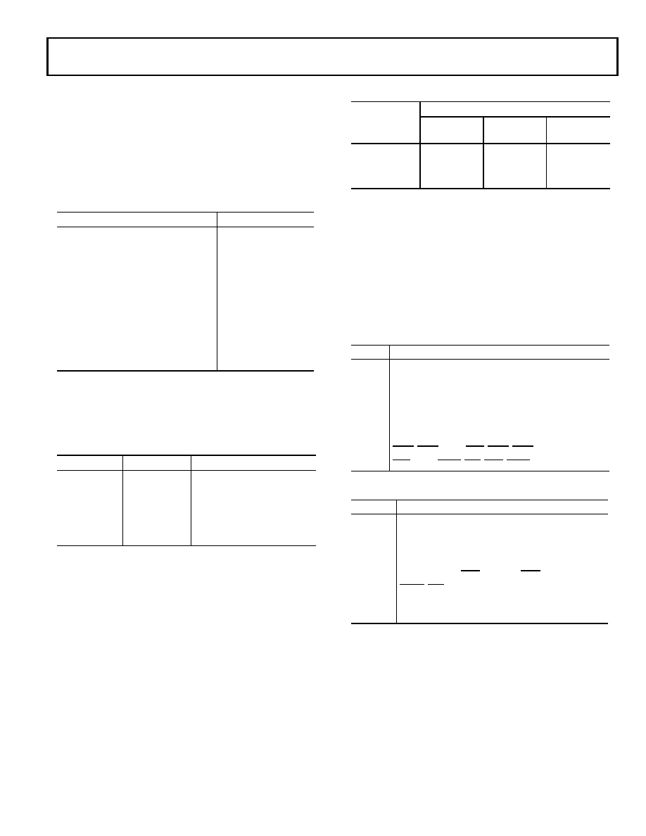
Table 17. Absolute Maximum Ratings
Parameter
Rating
Internal Supply Voltage (VDDINT)
– 0.3 V to +1.50 V
External (I/O) Supply Voltage
(VDDEXT/VDDMEM)
– 0.3 V to +3.8 V
Input Voltage
1, 2
1 Applies to 100% transient duty cycle. For other duty cycles see Table 18.
2 Applies only when VDDEXT is within specifications. When VDDEXT is outside speci-
fications, the range is VDDEXT ± 0.2.
–0.5 V to +3.6 V
Input Voltage1, 3
3 Applies to signals SCL, SDA.
–0.5 V to +5.5 V
Output Voltage Swing
– 0.5 V to
VDDEXT/VDDMEM+0.5 V
IOH/IOL Current per Pin Group
4
80 mA (max)
Storage Temperature Range
– 65°C to +150°C
Junction Temperature While biased
+110°C
Table 18. Maximum Duty Cycle for Input Transient Voltage1
1 Applies to all signal pins/balls with the exception of CLKIN, XTAL.
VIN Min (V)
2
2 The individual values cannot be combined for analysis of a single instance of
overshoot or undershoot. The worst case observed value must fall within one of
the voltages specified and the total duration of the overshoot or undershoot
(exceeding the 100% case) must be less than or equal to the corresponding duty
cycle.
VIN Max (V)
Maximum Duty Cycle3
3 Duty cycle refers to the percentage of time the signal exceeds the value for the
100% case. The is equivalent to the measured duration of a single instance of
overshoot or undershoot as a percentage of the period of occurrence.
–0.50
+3.80
100%
–0.70
+4.00
40%
–0.80
+4.10
25%
–0.90
+4.20
15%
–1.00
+4.30
10%
Table 19. Maximum OTP Memory Programming Time
Temperature
VPPOTP
Voltage (V)
25°C
85°C
110°C
6.9
6000 sec
100 sec
25 sec
7.0
2400 sec
44 sec
12 sec
7.1
1000 sec
18 sec
4.5 sec
Table 20. Total Current Pin Groups–VDDMEM Groups
Group
Pins in Group
1
DATA15, DATA14, DATA13, DATA12, DATA11, DATA10
2
DATA9, DATA8, DATA7, DATA6, DATA5, DATA4
3
DATA3, DATA2, DATA1, DATA0, ADDR19, ADDR18
4
ADDR17, ADDR16, ADDR15, ADDR14, ADDR13
5
ADDR12, ADDR11, ADDR10, ADDR9, ADDR8, ADDR7
6
ADDR6, ADDR5, ADDR4, ADDR3, ADDR2, ADDR1
7ABE1, ABE0, SA10, SWE, SCAS, SRAS
8SMS, SCKE, AMS1, ARE, AWE, AMS0, CLKOUT
Table 21. Total Current Pin Groups–VDDEXT Groups
Group
Pins in Group
1
PF9, PF8, PF7, PF6, PF5, PF4, PF3, PF2
2
PF1, PF0, PG15, PG14, PG13, PG12, PG11, PG10
3
PG9, PG8, PG7, PG6, PG5, PG4, PG3, PG2, BMODE0,
BMODE1, BMODE2
4PG1, PG0, TDO, EMU, TDI, TCK, TRST, TMS
5RESET, NMI, CLKBUF
6
PH7, PH6, PH5, PH4, PH3, PH2, PH1, PH0
7
PF15, PF14, PF13, PF12, PF11, SDA, SCL, PF10
相关PDF资料 |
PDF描述 |
|---|---|
| 2300HT-471-H-RC | INDUCTOR TOROID 470UH 15% HORZ |
| CS48560-CQZR | IC DSP HP 32BIT 12CH I/O 48-QFP |
| MAX7502MUA+T | IC TEMP SENSOR DIGIT 8-UMAX |
| MAX7503MSA+ | IC TEMP SENSOR DIGIT 8-SOIC |
| TPSB476K010A0650 | CAP TANT 47UF 10V 10% 1210 |
相关代理商/技术参数 |
参数描述 |
|---|---|
| ADSP-BF514KSWZ-4 | 功能描述:IC DSP 16/32B 400MHZ LP 176LQFP RoHS:是 类别:集成电路 (IC) >> 嵌入式 - DSP(数字式信号处理器) 系列:Blackfin® 标准包装:2 系列:StarCore 类型:SC140 内核 接口:DSI,以太网,RS-232 时钟速率:400MHz 非易失内存:外部 芯片上RAM:1.436MB 电压 - 输入/输出:3.30V 电压 - 核心:1.20V 工作温度:-40°C ~ 105°C 安装类型:表面贴装 封装/外壳:431-BFBGA,FCBGA 供应商设备封装:431-FCPBGA(20x20) 包装:托盘 |
| ADSP-BF514KSWZ-4F4 | 功能描述:IC DSP 16/32B 400MHZ LP 176LQFP RoHS:是 类别:集成电路 (IC) >> 嵌入式 - DSP(数字式信号处理器) 系列:Blackfin® 标准包装:2 系列:StarCore 类型:SC140 内核 接口:DSI,以太网,RS-232 时钟速率:400MHz 非易失内存:外部 芯片上RAM:1.436MB 电压 - 输入/输出:3.30V 电压 - 核心:1.20V 工作温度:-40°C ~ 105°C 安装类型:表面贴装 封装/外壳:431-BFBGA,FCBGA 供应商设备封装:431-FCPBGA(20x20) 包装:托盘 |
| ADSP-BF516BBCZ-3 | 功能描述:IC DSP 16/32B 300MHZ 168CSPBGA RoHS:是 类别:集成电路 (IC) >> 嵌入式 - DSP(数字式信号处理器) 系列:Blackfin® 标准包装:2 系列:StarCore 类型:SC140 内核 接口:DSI,以太网,RS-232 时钟速率:400MHz 非易失内存:外部 芯片上RAM:1.436MB 电压 - 输入/输出:3.30V 电压 - 核心:1.20V 工作温度:-40°C ~ 105°C 安装类型:表面贴装 封装/外壳:431-BFBGA,FCBGA 供应商设备封装:431-FCPBGA(20x20) 包装:托盘 |
| ADSP-BF516BBCZ-4 | 功能描述:IC DSP 16/32B 400MHZ 168CSPBGA RoHS:是 类别:集成电路 (IC) >> 嵌入式 - DSP(数字式信号处理器) 系列:Blackfin® 标准包装:2 系列:StarCore 类型:SC140 内核 接口:DSI,以太网,RS-232 时钟速率:400MHz 非易失内存:外部 芯片上RAM:1.436MB 电压 - 输入/输出:3.30V 电压 - 核心:1.20V 工作温度:-40°C ~ 105°C 安装类型:表面贴装 封装/外壳:431-BFBGA,FCBGA 供应商设备封装:431-FCPBGA(20x20) 包装:托盘 |
| ADSP-BF516BBCZ-4F4 | 功能描述:IC DSP 16/32B 400MHZ 168CSPBGA RoHS:是 类别:集成电路 (IC) >> 嵌入式 - DSP(数字式信号处理器) 系列:Blackfin® 标准包装:2 系列:StarCore 类型:SC140 内核 接口:DSI,以太网,RS-232 时钟速率:400MHz 非易失内存:外部 芯片上RAM:1.436MB 电压 - 输入/输出:3.30V 电压 - 核心:1.20V 工作温度:-40°C ~ 105°C 安装类型:表面贴装 封装/外壳:431-BFBGA,FCBGA 供应商设备封装:431-FCPBGA(20x20) 包装:托盘 |
发布紧急采购,3分钟左右您将得到回复。